— FREE — Schottky Barrier
Header
- Files for the tutorial located in nextnano++\examples\basics:
contacts_1D_ohmic_charge_neutral_GaAs_nnp.in
contacts_1D_schottky_barrier_GaAs_nnp.in
contacts_2D_schottky_barrier_GaAs_nnp.in (not compatible with the free version)
- Scope:
The Schottky barrier at the boundary of simulation domain.
Introduction
When a metal is in contact with a semiconductor, a potential barrier is formed at the metal-semiconductor interface. In 1938, Walter Schottky suggested that this potential barrier arises due to stable space charges in the semiconductor. At thermal equilibrium, the Fermi levels of the metal and the semiconductor must coincide. There are two limiting cases:
Ideal Schottky barrier:
metal/n-type semiconductor: The barrier height \(\phi_B\) is the difference of the metal work function \(\phi_M\) and the electron affinity (\(\chi\)) in the semiconductor.
\[\mathrm{e} \phi_B = \mathrm{e} ( \phi_M - \chi_s )\]
metal/p-type semiconductor: The barrier height \(\phi_{B,p}\) is given by:
\[\mathrm{e} \phi_{B,p} = \mathrm{e} ( \phi_M - \chi_s ) - E_\mathrm{gap}\]Fermi level pinning:
If surface states on the semiconductor surface are present: The barrier height is determined by the property of the semiconductor surface and is independent of the metal work function
Consequently, the Schottky barrier corresponds a (Dirichlet) boundary condition for the electrostatic potential, i.e. the solution of the Poisson equation in the semiconductor, because the conduction and valence band edge energies are in a definite energy relationship with the Fermi level of the metal.
The Schottky barrier model implemented in nextnano++ corresponds to pinning of the Fermi level and does not take into account the work function of the metal. Due to such definition, the barrier height is independent of the metal work function and is entirely determined by the surface states and the doping.
contacts{
    schottky{                   # Schottky barrier (Fermi level pinning)
        name = contact
        bias = 0.0              # [V] apply voltage
        barrier = 0.53          # [V] GaAs, S.M. Sze, "Physics of Semiconductor Devices", p. 275 (2nd ed.)
    }
}
Schottky Barrier
All input files in this tutorial assume n-type donor concentration in \(GaAs\) has to be 1 \(\cdot\) 1019 cm-3 with realistic activation energies. With the temperature set to 300 K this effects in having the Fermi level in the conduction band of the n-doped GaAs, see bandedges.dat output by contacts_1D_ohmic_charge_neutral_GaAs_nnp.in.
Running the contacts_1D_ohmic_charge_neutral_GaAs_nnp.in and contacts_1D_schottky_barrier_GaAs_nnp.in with the $barrier=0.53 and $barrier=0.00 one can obtain a comparison of band profiles as presented in the Figure 2.4.2.29, which shows the conduction band edge profile for n-type \(GaAs\) in equilibrium with
the Schottky barrier of 0.53 V, i.e. the conduction band edge is pinned 0.53 eV above the Fermi level set at 0 eV
the Schottky barrier of 0.00 V
no barrier within “ohmic” contact
at position of 10 nm. The contact regions in these simulations are defined in the range from 0 nm to 10 nm but no equations are solved inside this region as both Fermi levels and electric potential are already assumed there as boundary conditions.
Note that in equilibrium the Fermi level is constant and equal to 0 eV in the whole device. If the semiconductor is doped, the conduction and valence band edges are shifted with respect to this Fermi level, i.e. relative to 0 eV and are thus dependent on doping. This is a bulk property and independent of surface effects, like ohmic contacts or Schottky barrier height, see right end of the Figure 2.4.2.29. At the left boundary, however, the band profile is affected by the type of contact.
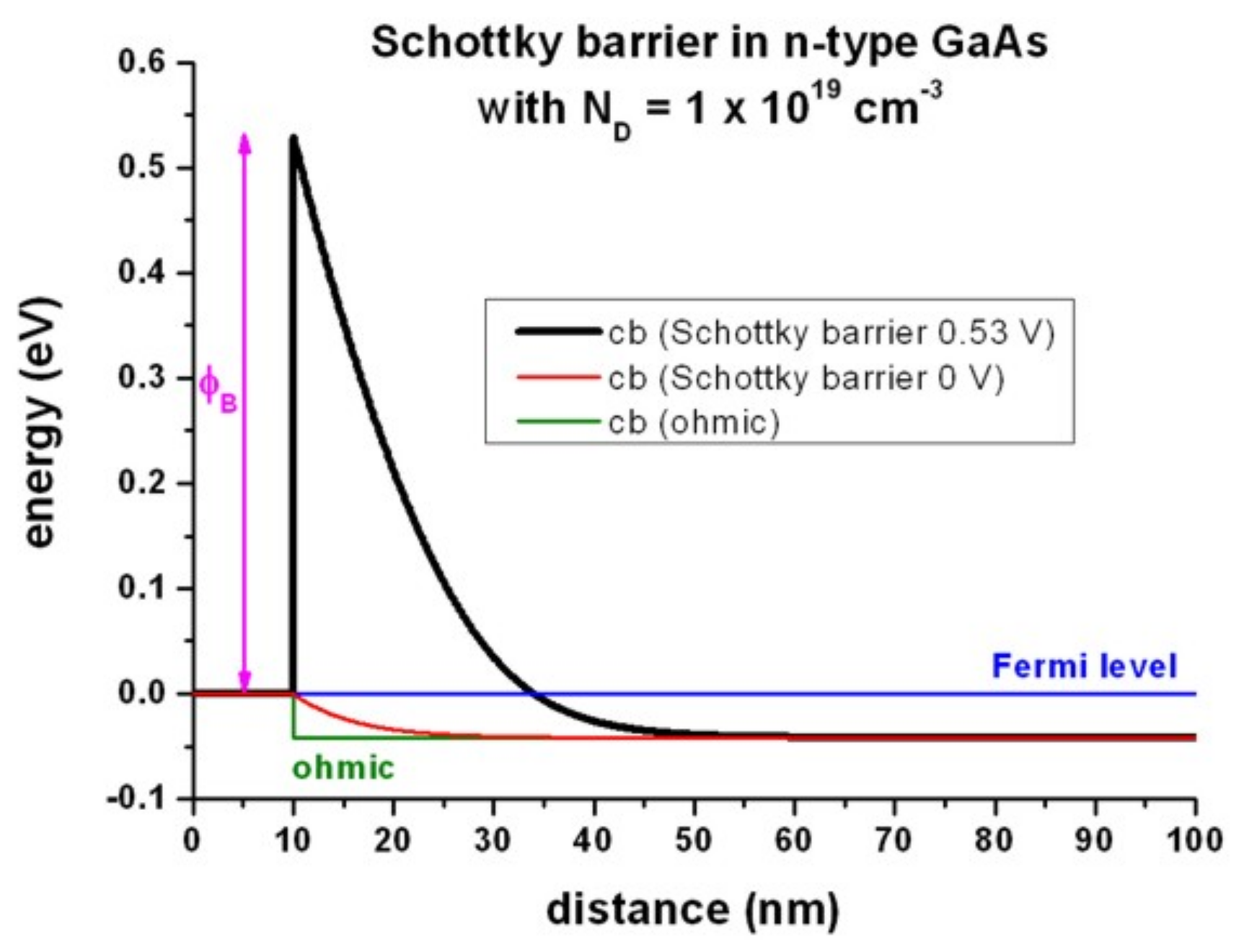
Figure 2.4.2.29 Calculated conduction band profile
Note
A Schottky barrier of 0 V is not equivalent to an ohmic contact.
Both contacts{ schottky{} } and contacts{ ohmic{} } used in the input files poses Dirichlet boundary conditions for the Poisson and Current equations.
Within the contacts{ ohmic{} }, the electrostatic potential is set to the value satisfying requirement of charge neutrality in the region of this contact, \(\phi=0\).
The contacts{ schottky{} } in the input files sets this value by the Schottky barrier, \(\phi_B\), being the value of the conduction band edge at the boundary with respect to the Fermi level:
In this particular example, an artificial Schottky barrier of -0.0365 V would be an equivalent to results obtained using an contacts{ ohmic{} }, (i.e. flat band condition), but only for the same temperature and the same doping concentration.
The input file contacts_2D_schottky_barrier_GaAs_nnp.in shows how to obtain the same results within 2D simulation.
Last update: 16/07/2024