Hexagonal GaAs/AlGaAs nanowires
- Input files:
2DGaAs_AlGaAs_circle_nnp.in
2DGaAs_AlGaAs_hexagon_nnp.in
2D_Hexagonal_Nanowire_2DEG_nnp.in
- Scope:
In this tutorial we simulate a circular and a hexagonal \(GaAs/Al_{0.33}Ga_{0.67}As\) core-shell structure (Part A) and a hexagonal \(GaAs/AlGaAs\) nanowire structure (Part B).
- Output files:
bias_00000\Quantum\probabilities_quantum_region_Gamma_.vtr
Part A: Schrödinger equation of a two-dimensional core-shell structure
In this part of the tutorial, we solve the two-dimensional Schrödinger equation of a circular and a hexagonal \(GaAs/Al_{0.33}Ga_{0.67}As\) core-shell structure.
Circular core-shell structure
Input file: 2DGaAs_AlGaAs_circle_nnp.in
Figure 2.4.7.1 shows the probability density of the 6th eigenstate of the circular \(GaAs/ AlGaAs\) structure. The data is contained in the file bias_00000\Quantum\probabilities_quantum_region_Gamma_.vtr. It’s energy level is higher than the \(AlGaAs\) barrier energy, i.e. this state is not confined in the circular shaped \(GaAs\) quantum well. The horizontal and vertical slices are through the center and show the square of the probability amplitude of this eigenstate.
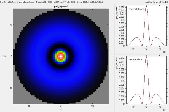
Figure 2.4.7.1 \(\Psi^2\) of the 6th electron eigenstate.
The \(GaAs\) core has a radius of 5 nm. (It cannot be recognized on this plot.) The \(AlGaAs\) shell has a radius of 15 nm. It is surrounded by an infinite barrier which comes from the “band offset” due to the surrounding material “air”.
Hexagonal core-shell structure
Input file: 2DGaAs_AlGaAs_hexagon_nnp.in
Figure 2.4.7.2 shows the conduction band edge of the hexagonal \(GaAs/ AlGaAs\) structure. The \(GaAs\) region is indicated in black, the \(AlGaAs\) region in blue. Horizontal and vertical slices through the center show the energy of the conduction band edge profile. The data is contained in the file bias_00000\bandedges.fld
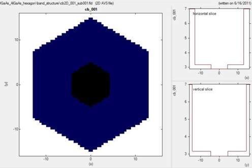
Figure 2.4.7.2 Conduction band edge profile of the hexagonal core-shell structure.
The diameter of the hexagonal shaped \(GaAs\) core is ~8.66 nm (corresponding to an outer radius of the core of 5 nm), and the diameter of the hexagonal shaped \(AlGaAs\) shell is ~26 nm (corresponding to an outer radius of the shell of 15 nm).
Figure 2.4.7.3 shows the probability density of the 10th eigenstate of the circular \(GaAs/ AlGaAs\) structure. The data is contained in the file bias_00000\Quantum\probabilities_quantum_region_Gamma_.vtr. It’s energy level is higher than the \(AlGaAs\) barrier energy, i.e. this state is not confined in the hexagonal shaped \(GaAs\) quantum well. The horizontal and vertical slices are through the center and show the square of the probability amplitude of this eigenstate.
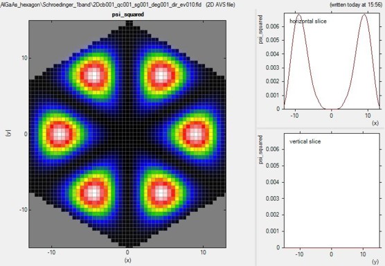
Figure 2.4.7.3 \(\Psi^2\) of 10th electron eigenstate.
The hexagonal \(GaAs\) core has an outer radius of 5 nm. It cannot be seen on this plot. The \(AlGaAs\) shell has a diameter of 26 nm. It is surrounded by an infinite barrier which case comes from the “band offset” due to the surrounding material “air”.
Alloy sweep
Note
In comparison with nextnano³, nextnano++ does not support an alloy sweep in the input file. However, you can use nextnanomat’s Template feature to perform an alloy sweep.
In the following, we vary the alloy content \(x\) of the ternary \(Al_xGa_{1-x}As\) from 0 to 0.33 in 11 steps. For \(x\) = 0, we have pure \(GaAs\). For \(x\) = 0.33 we have an \(AlGaAs/GaAs\) conduction band offset of 0.285 eV, and a valence band offset of -0.168 eV. In the latter case, the quantum confinement is stronger. Even for \(x\) = 0 we have “quantum confinement” due to the Dirichlet boundary conditions (corresponding to infinite barriers) at the shell surface that we use for the Schrödinger equation. Consequently, even for \(x\) = 0, we get an e1 - h1 transition energy from the lowest electron state (e1) to the highest heavy hole state (h1) that is larger than the band gap as shown in Figure 2.4.7.4.
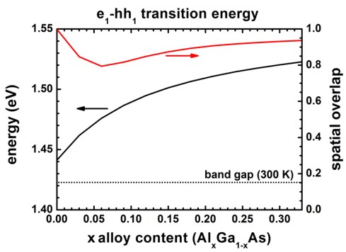
Figure 2.4.7.4 Transition energy and spatial overlap of e1 to h1 transition as a function of alloy content \(x\).
The transition energies (e1 - h1), as well as the spatial overlap integral of the electron and hole ground state wave functions, are contained in this file: bias_00000\Quantum\intraband_matrix_elements_quantum_region_Gamma_001.txt
alloy      type                         el-hl[eV]     el[eV]        hl[eV]        matrix_element
0.330000   |<psi_vb001|psi_cb001_>|^2   1.522777615   2.965889676   1.443112062   0.936344908
0.300000   |<psi_vb001|psi_cb001_>|^2   1.520316794   2.963669699   1.443352905   0.931291593
...
The spatial overlap of electron and hole wave functions is always very high. When there is only confinement due to the shell boundary, the matrix element is very high (99.8 %). The matrix element must be smaller than 1 for \(x\) = 0 because the electron and hole masses are different. The matrix element must be even smaller (94 %) for \(x\) = 0.33 (strong confinement) because in addition to the mass difference, the conduction and valence band offsets are not equivalent. The matrix element has a minimum at around \(x\) = 0.06 because in this case the electron wave function penetrates into the barrier much stronger that the hole wave function does. Thus the differences in well and barrier masses (as well as band offsets) play an important role for the spatial extension of the wave functions.
Part B: Hexagonal 2DEG - Two-dimensional electron gas in a delta-doped hexagonal shaped \(GaAs/AlGaAs\) nanowire heterostructure
Input file: 2D_Hexagonal_Nanowire_2DEG_nnp.in
The following example deals with a delta-doped \(GaAs/AlGaAs\) 2DEG (two-dimensional electron gas) structure. In this case, the heterostructure consists of a hexagonal \(GaAs/AlGaAs\) nanowire, see Figure 2.4.7.5.
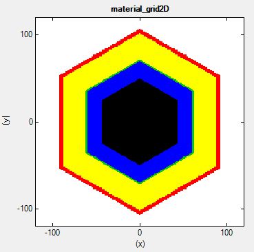
Figure 2.4.7.5 The material layers of the struture: \(GaAs\) core (black), \(AlGaAs\) spacer (blue), Si-doped \(AlGaAs\) (green), \(AlGaAs\) (yellow), \(GaAs\) capping layer (red) and Schottky barrier contact (black) are shown. (The white layer itself is not included in the calculation. It only serves as a boundary condition)
The self-consistently calculated conduction band edge (bandedges.fld) is shown in Figure 2.4.7.6. The horizontal and vertical slices through the center indicate the triangular potential well (conduction band minimum) where the 2DEG is located.
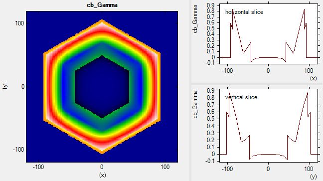
Figure 2.4.7.6 Conduction band edge profile.
The resulting 2DEG electron density (bias_00000\density_electron_fld) is shown Figure 2.4.7.7. At the corners, the electron density is significantly higher, thus one-dimensional conducting channels are formed. Although the structure itself has a hexagonal symmetry, our rectangular grid breaks this symmetry. Therefore the density in the upper/lower corner are different from the density at the left/right corners.
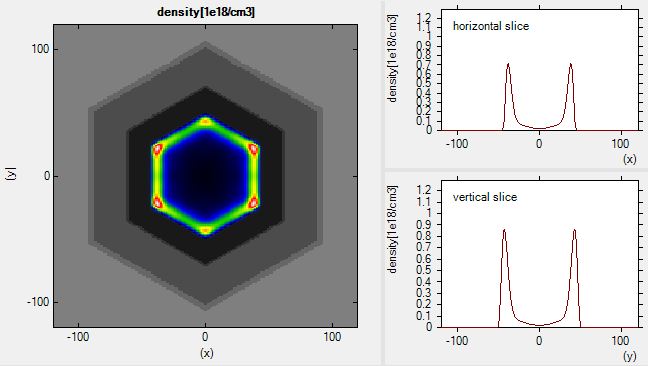
Figure 2.4.7.7 Charge density profile.
The 2D Poisson equation and the 2D Schrödinger equation have been solved self-consistently. The dimension of the Schrödinger matrix is 28,625. The CPU time for this calculation was about 18 minutes.
Last update: nn/nn/nnnn