— FREE — GaAs p–n junction
Author Stefan Birner
Note
See a tutorial on IV curves for pn junctions described here
- Input Files:
pn_junction_GaAs_1D_nnp.in
pn_junction_GaAs_2D_nnp.in
pn_junction_GaAs_3D_nnp.in
This tutorial discusses the nextnano++ input file. Identical results can be achieved with the nextnano³ input files listed above.
This tutorial aims to reproduce Figure 3.1 (p. 51) of Joachim Piprek’s book “Semiconductor Optoelectronic Devices - Introduction to Physics and Simulation” (Section 3.2 “pn-junctions”)
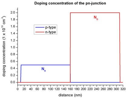
Doping concentration
The structure consists of 300 nm GaAs. At the left and right boundaries, metal contacts are connected to the GaAs semiconductor (i.e. from 0 nm to 10 nm, and from 310 nm to 320 nm). The structure is p-type doped from 10 nm to 160 nm and n-type doped from 160 nm and 310 nm.
The following figure shows the concentration of donors and acceptors of the p-n junction. In the p-type region between 10 nm and 160 nm, the number of acceptors, \(N_A\) is \(0.5 \times 10^{18}\) cm-3 In the n-type region between 160 nm and 310 nm, the number of donors, \(N_D\) is \(2.0 \times 10^{18}\) cm-3
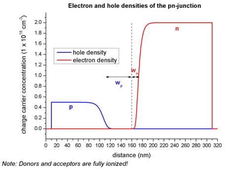
Carrier concentrations
The equilibrium condition for a p-n junction is achieved by a small transfer of electrons from the n region to the p region, where they recombine with holes. This leads to a depletion region (depletion width = \(w_p + w_n\)), i.e. the region around the p-n junction only has very few free carriers left. The following figure shows the electron and hole densities and the depletion region around the p-n junction at 160 nm. Here, we assumed that all donors and acceptors are fully ionized.
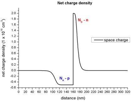
Net charges (space charge)
In the depletion region, a net charge results from the ionized donors \(N_D\) and ionized acceptors \(N_A\). The following figure shows the net charge density of the p-n junction.
Electric field
The slope of the electric field is proportional to the net charge (Poisson equation), thus the extremum of the electric field is expected to be at the p-n junction. In regions without charges, the electric field is zero. The following figure shows the electric field of the p-n junction.
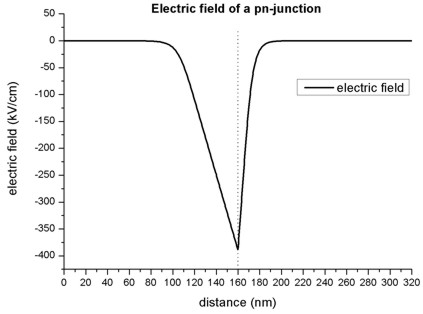
The extremum of the electric field \(F_{max}\) (at 160 nm) can be approximated as follows:
Symbol |
Value |
|---|---|
e |
\(1.6022 \times 10^{-19} \text{As}\) |
\(\epsilon\) |
12.93 (Dielectric constant of GaAs) |
\(\epsilon_0\) |
\(8.854 \times 10^{12} \text{As/(Vm)}\) |
\(N_A\) |
\(0.5 \times 10^{18} \text{cm}^{-3}\) |
\(N_D\) |
\(2.0 \times 10^{18} \text{cm}^{-3}\) |
\(w_p\) |
55.3 nm |
\(w_n\) |
13.8 nm |
Electrostatic potential, conduction and valence band edges
In regions, where the electric field is zero, the electrostatic potential is constant. The electrostatic potential phi determines the conduction and valence band edges:
\(E_c=E_{c0}-e\phi\)
\(E_v=E_{v0}-e\phi\)
The following figure shows the conduction and valence band edges, the electrostatic potential and the Fermi level of the p-n junction.
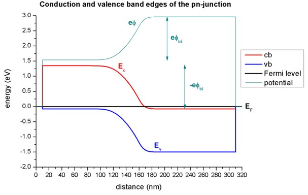
Without external bias (i.e. equilibrium), the Fermi level \(E_F\) is constant (\(E_F=0 \space \text{eV}\)).
The built-in potential \(\phi_{bi}\) was calculated by nextnano++ to be equal to 1.426 V It can be approximated as follows:
Assuming \(F_{\text{max}} = 387 \text{kV/cm}\), this would result in a depletion width: \(w_p + w_n = 73.7 \text{nm}\)
To allow for a constant chemical potential (i.e. constant Fermi level \(E_F\)), a total potential difference of \(-e \phi_{bi}\) is required.
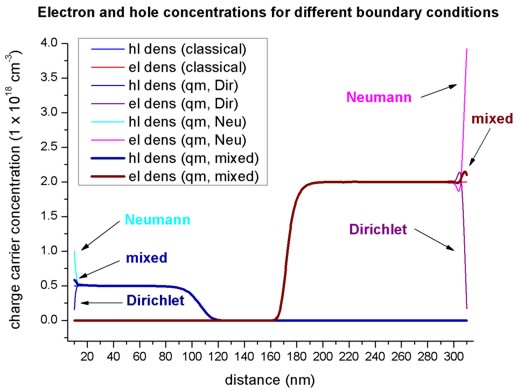
Quantum mechanical solution
Using the nextnano³ input file pn_junction_GaAs_1D_QM_nn3.in, we can solve the Schrödinger equation for the electrons, light and heavy holes in the single-band approximation over the whole device, rather than classically. We calculate up to 300 eigenvalues for each band. Thus the electron and hole densities are calculated purely quantum mechanically. The following figure shows the electron and hole concentrations for the classical and quantum mechanical calculations. For the QM calculations, different boundary conditions were used.
Dirichlet boundary conditions force the wave functions to be zero at the boundaries, thus the density goes to zero at the boundaries which is unphysically.
Neumann boundary conditions lead to unphysically large values at the boundaries.
For the classical calculation, the densities at the boundaries are constant. Nevertheless, in the interesting region around the p-n junction, all four options lead to identical densities.
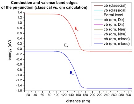
The following figure shows the band edges of the p-n junction for the four cases:
Classical calculation
Quantum mechanical calculation with Dirchlet boundary conditions
Quantum mechanical calculation with Neumann boundary conditions
Quantum mechanical calculation with mixed boundary conditions (this feature is no longer supported)
For all cases the band edges are identical in the area around the p-n junction. Tiny deviations exist at the boundaries of the device.
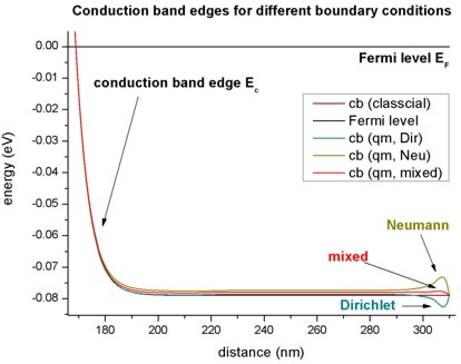
This figure is a zoom into the right boundary of the conduction band edge. On this scale, the tiny deviations for the different boundary conditions can be clearly seen.
Non-equilibrium
So-called “quasi-Fermi levels” which are different for electrons (\(E_F\), \(n\)) and holes (\(E_F\), \(p\)) are used to describe nonequilibrium carrier concentrations.
In equilibrium the quasi-Fermi levels are constant and have the same value for both electrons and holes (\(E_{Fn} = E_{Fp} = 0 \space \text{eV}\)). The current is proportional to the mobility and the gradient of the quasi-Fermi level \(E_F\).
2D/3D Simulations
pn_junction_GaAs_2D_nn3.in / *_nnp.in - input file for the nextnano³ and nextnano++ tools
pn_junction_GaAs_3D_nn3.in / *_nnp.in - input file for the nextnano³ and nextnano++ tools
These input files are for the same p-n junction structure as in the 1D case, but extended into 2D and 3D.
2D: rectangle of dimension 320 nm x 200 nm
3D: cuboid of dimension 320 nm x 200 nm x 100 nm
Complete input file for nextnano++
#***************************************************************************!
#                                                                           !
# pn_junction_GaAs_1D_nnp.in                                                !
# --------------------------                                                !
#                                                                           !
# This is an input file for nextnano++ to calculate the band edges of a     !
# simple p-n junction with classical charge densities.                       !
#                                                                           !
# It's part of the 1D p-n junction tutorial which can be found at:           !
# https://www.nextnano.com/nextnano3/tutorial/1Dtutorial_pn_junction.htm     !
#                                                                           !
# For help on the individual keywords please go to                          !
# https://www.nextnano.com/nextnanoplus/software_documentation/input_file.htm !
#                                                                           !
# nextnano (c) nextnano GmbH                                                !
# This input file is (c) Stefan Birner, nextnano GmbH.                      !
# This file is protected by applicable copyright laws. You may use it       !
# within your research or work group, but you are not allowed to give       !
# copies to other people without explicit permission.                       !
#                                                                           !
# Documentation: https://www.nextnano.com/nextnanoplus/                     !
# Support:       support@nextnano.com                                       !
#***************************************************************************!


global{
simulate1D{}

temperature = 300.0                                                    # Kelvin

substrate{ name = "GaAs" }

crystal_zb{
        x_hkl = [1, 0, 0]
        y_hkl = [0, 1, 0]
}
}

grid{
#
# For consistency reasons, we use the same nonuniform grid spacing as the nextnano3 input file.
# However, using jumps in the grid spacing (e.g. at x=100.0 where the grid spacing changes abruptly)
# is not a good practice, as numerical errors increase.
#
xgrid{
        line{ pos = 0.0       spacing = 2.0  }
        line{ pos = 10.0      spacing = 2.0  }
        line{ pos = 10.0      spacing = 1.0  }
        line{ pos = 100.0     spacing = 1.0  }
        line{ pos = 100.0     spacing = 0.5  }
        line{ pos = 140.0     spacing = 0.5  }
        line{ pos = 140.0     spacing = 0.25 }
        line{ pos = 180.0     spacing = 0.25 }
        line{ pos = 180.0     spacing = 0.5  }
        line{ pos = 220.0     spacing = 0.5  }
        line{ pos = 220.0     spacing = 1.0  }
        line{ pos = 310.0     spacing = 1.0  }
        line{ pos = 310.0     spacing = 2.0  }
        line{ pos = 320.0     spacing = 2.0  }
}
}

structure{
output_region_index{ boxes = no }
output_material_index{ boxes = no }
output_alloy_composition{ boxes = no }
output_impurities{ boxes = no }

region{
        everywhere{}
        binary{ name = "GaAs" }
}
region{
        line{
                x = [0.0, 10.0]
        }
        binary{
                name = "GaAs"
        }
        contact { name = source }
}
region{
        line{
                x = [10.0, 310.0]
        }
        binary{
                name = "GaAs"
        }
}
region{
        line{
                x = [310.0, 320.0]
        }
        binary{
                name = "GaAs"
        }
        contact { name = drain }
}

region{
        line{
                x = [ 0.0, 160.0]
        # x = [10.0, 160.0]     # doping must not start at 10.0
        }
        doping{
                constant{
                        name = "p-type"
                        conc =  0.5e18
                }
        }
}

region{
        line{
        # x = [160.0, 310.0]    # doping must not end at 310.0
                x = [160.0, 320.0]
        }
        doping{
                constant{
                        name = "n-type"
                        conc = 2.0e18
                }
        }
}
}

impurities{
#    donor{ name = "n-type" energy = 0.027   degeneracy = 2 }
# acceptor{ name = "p-type" energy = 0.0058  degeneracy = 4 }
        donor{ name = "n-type" energy = -1000.0 degeneracy = 2 }    # '-1000.0' eV = all ionized
acceptor{ name = "p-type" energy = -1000.0 degeneracy = 4 }    # '-1000.0' eV = all ionized
}

contacts{
ohmic{ name = "source" bias = 0.0 }
ohmic{ name = "drain"  bias = 0.0 }
}

classical{
Gamma{}
HH{}
LH{}
SO{}

output_bandedges{ averaged = no}
output_carrier_densities{}
output_ionized_dopant_densities{}
output_intrinsic_density{}
}

poisson{
output_potential{}
output_electric_field{}
}

run{
solve_poisson{ }
}
- Input Files for nextnano³:
pn_junction_GaAs_1D_nn3.in
pn_junction_GaAs_1D_QM_nn3.in
pn_junction_GaAs_2D_nn3.in
pn_junction_GaAs_3D_nn3.in
Last update: nn/nn/nnnn