Quantum-Cascade Lasers
- Input files:
examples\quantum_cascade_lasers\1DQuantumCascadeLaser_nnp.in
examples\quantum_cascade_lasers\1DQuantumCascadeLaserSiGe_nnpp.in
examples\quantum_cascade_lasers\1DQCL_AlGaAs_Sirtori_APL73_1998_nnp.in
examples\quantum_cascade_lasers\1DQCL_Andrea_Friedrich_NoInjector_InGaAs_APL86_2005_kp_nnp.in
examples\quantum_cascade_lasers\1DQCL_Andrea_Friedrich_NoInjector_InGaAs_APL86_2005_sg_nnp.in
examples\quantum_cascade_lasers\1DQCL_Rochat_APL81_2002_nnp.in
examples\quantum_cascade_lasers\1DQCL_THz_MIT_Sandia_SemicScTech20_2005_nnp.in
examples\quantum_cascade_lasers\THzQCL_Andrews_Vienna_MatSciEng2008_nnp.in
examples\quantum_cascade_lasers\THzQCL_Andrews_Vienna_MatSciEng2008_nnp_electric_field.in
examples\quantum_cascade_lasers\THzQCL_Andrews_Vienna_MatSciEng2008_nnp_no_repeat.in
Note
If you want to obtain the input files that are used within this tutorial, please check if you can find them in the installation directory. If you cannot find them, please submit a Support Ticket.
- Scope:
This tutorial aims to simulate different quantum-cascade structures proposed in the literature.
GaAs/ AlGaAs Quantum-Cascade Laser
This tutorial is based on the quantum-cascade structure that has been presented in [Page2001]. Here, we are trying to reproduce fig. 1 of this paper. The corresponding input file is 1DQuantumCascadeLaser.in.
The quantum-cascade structure consists of a sequence of \(GaAs\) wells and \(Al_{0.45}Ga_{0.55}As\) barriers. The sequence is as follows (from 0 nm to 45 nm; it is repeated outside this region):
Layer |
Thickness [nm] |
|
1 |
\(Al_{0.45}Ga_{0.55}As\) |
4.6 |
2 |
\(GaAs\) |
1.9 |
3 |
\(Al_{0.45}Ga_{0.55}As\) |
1.1 |
4 |
\(GaAs\) |
5.4 |
5 |
\(Al_{0.45}Ga_{0.55}As\) |
1.1 |
6 |
\(GaAs\) |
4.8 |
7 |
\(Al_{0.45}Ga_{0.55}As\) |
2.8 |
8 |
\(GaAs\) |
3.4 |
9 |
\(Al_{0.45}Ga_{0.55}As\) |
1.7 |
10 |
\(GaAs\) |
3.0 |
11 |
\(Al_{0.45}Ga_{0.55}As\) |
1.8 |
12 |
\(GaAs\) |
2.8 |
13 |
\(Al_{0.45}Ga_{0.55}As\) |
2.0 |
14 |
\(GaAs\) |
3.0 |
15 |
\(Al_{0.45}Ga_{0.55}As\) |
2.6 |
16 |
\(GaAs\) |
3.0 |
In [Page2001], a conduction band offset of 390 meV was used. Consequently, we modify our default band offset by shifting the AlGaAs ternary to get a 390 meV offset. We also apply an electric field of -48 kV/cm.
$ElectricField      = 48e5    # Electric field in units of [V/m] - Here: 48 kV/cm
$ReferencePotential = 0.092   # Set the potential at the leftmost point of the grid to the same value as in nextnano3
For simplicity, in contrast to [Page2001], we do not include doping here. In the original paper, the areas between 15.2 nm and -5.6 nm (9.8 nm) and 29.8 nm and 39.4 nm (9.8 nm), corresponding to layer 11 - 14, were n-type doped with silicon, with a sheet density of \(n_\mathrm{Si}\) = 3.8 \(\cdot\) 1011 cm-2. In this example, we do not have to calculate the strain, because piezo and any pyroelectric fields do not exist. We use single-band (effective-mass) rather than 8-band k.p model.
Bandedge profile
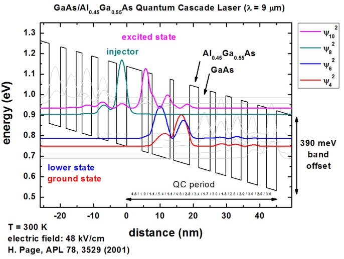
Figure 2.4.11.1 Calculated conduction band edge (black line) of the quantum-cascade structure with electric field of strength 48 kV/cm applied. Also shown are the probability densities (\(\Psi^2\)) of four electron states, which are shifted by their corresponding eigenenergies.
Figure 2.4.11.1 shows the conduction band energy of the Gamma conduction band edge and the probability densities (\(\Psi^2\)) of the ground state 4 (red), the lower state 6 (blue), the excited state 10 (pink) and the injector state 8 (green). The above shown structure of the conduction band edge and the wave functions is in excellent agreement with fig. 1 of [Page2001].
Note that periodic boundary conditions for the Schrödinger and Poisson equation do not make sense because of the application of an electric field. Thus, we used Dirichlet boundary conditions. However, this will lead to some artificial, wrong wave functions at the boundaries because the wave function is forced to be zero at the boundaries. For the states in the middle of the device where the wave function decays to zero in any case at the boundaries, the boundary conditions do not have any influence at all and so these states are fine. So the suggestion is to calculate 3 or 5 periods, and then take the energy levels and wave functions of the center period. In this way, boundary effects should not be very severe.
global{
    periodic{ x = yes }  # apply period boundary conditions along the x-direction
}
Intraband matrix elements
The files:
bias_00000\Quantum\interband_matrix_elements_qr1_Gamma_100.txt
bias_00000\Quantum\dipole_moment_matrix_elements_qr1_Gamma_100.txt
contain the \(p_x\) and \(z\) intraband matrix elements for all transitions. Our result for the \(z\) matrix element for the transition between the excited state to lower state is in excellent agreement with the result of [Page2001]:
\(\left\langle\Psi_{10}|z|\Psi_6\right\rangle\) |
\(z_{10,6}\) = 1.6655138016 nm |
\(z_{3,2}\) = 1.7 nm |
\(\Delta E_\mathrm{transition}\) |
147.7 meV |
160 meV |
QCL examples
Note
Please submit a support ticket if you want to obtain the input files for the following structures.
1. \(\lambda\) = 9 \(\mathrm{\mu}\)m, i.e. 33 THz or 138 meV
The simulated QCL structure is taken from [Page2001], see Figure 2.4.11.1. The corresponding input is 1DQuantumCascadeLaser.in.
2. \(\lambda\) = 9.4 \(\mathrm{\mu}\)m or 132 meV
The simulated quantum-cascade structure, shown in Figure 2.4.11.2, is based on [Sirtori1998]. The corresponding input file is 1DQCL_AlGaAs_Sirtori_APL73_1998.in.
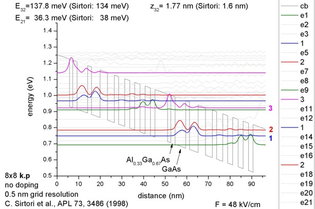
Figure 2.4.11.2 Calculated conduction band edge (black line) of the quantum-cascade structure with electric field of strength 48 kV/cm applied. Also shown are the probability densities (\(\Psi^2\)) of several electron states, which are shifted by their corresponding eigenenergies.
3. \(\lambda\) = 10 \(\mathrm{\mu}\)m or 124 meV (77 K)
The simulated quantum-cascade structure, shown in Figure 2.4.11.3 and Figure 2.4.11.4, is based on [Friedrich2005]. The corresponding input file is 1DQCL_Andrea_Friedrich_NoInjector_InGaAs_APL86_2005_kp.in.
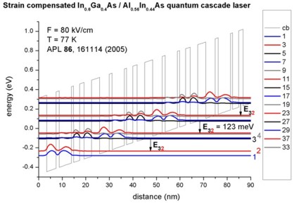
Figure 2.4.11.3 Calculated conduction band edge (black line) of the quantum-cascade structure with electric field of strength 80 kV/cm applied (\(T\) = 77 K). Also shown are the probability densities (\(\Psi^2\)) of several electron states, which are shifted by their corresponding eigenenergies.
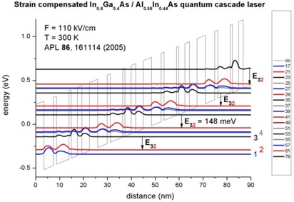
Figure 2.4.11.4 Calculated conduction band edge (black line) of the quantum-cascade structure with electric field of strength 110 kV/cm applied (\(T\) = 300 K). Also shown are the probability densities (\(\Psi^2\)) of several electron states, which are shifted by their corresponding eigenenergies.
4. \(\lambda\) = 66 \(\mathrm{\mu}\)m, i.e. 4.54 THz or 18.8 meV
The simulated quantum-cascade structure, shown in Figure 2.4.11.5, is based on [Rochat2002]. The corresponding input file is 1DQCL_Rochat_APL81_2002.in.
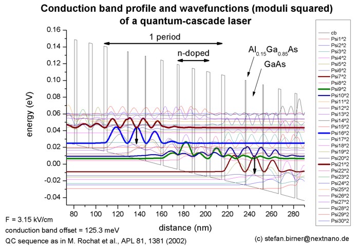
Figure 2.4.11.5 Calculated conduction band edge (black line) of the quantum-cascade structure with electric field of strength 3.15 kV/cm applied. Also shown are the probability densities (\(\Psi^2\)) of several electron states, which are shifted by their corresponding eigenenergies.
5. \(\lambda\) = 89.2 \(\mathrm{\mu}\)m, i.e. 3.4 THz or 13.9 meV
The simulated quantum-cascade structure, shown in Figure 2.4.11.6, is based on [Hu2005]. The corresponding input file is 1DQCL_THz_MIT_Sandia_SemicScTech20_2005.in.
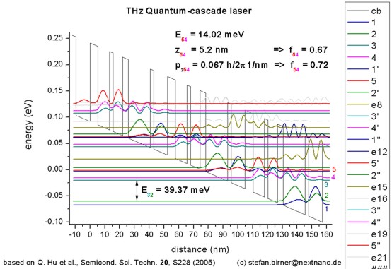
Figure 2.4.11.6 Calculated conduction band edge (black line) of the quantum-cascade structure with electric field of strength 12.2 kV/cm applied. Also shown are the probability densities (\(\Psi^2\)) of several electron states, which are shifted by their corresponding eigenenergies.
6. \(\lambda\) = 107 \(\mathrm{\mu}\)m, i.e. 2.8 THz or 11 meV
The simulated quantum-cascade structure, shown in Figure 2.4.11.7, is based on [Andrews2008]. The corresponding input file is THzQCL_Andrews_Vienna_MatSciEng2008_nnp.in.
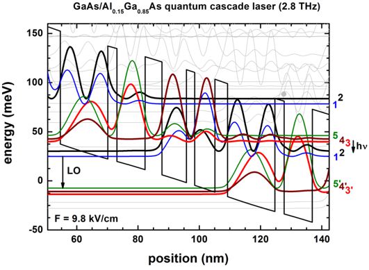
Figure 2.4.11.7 Calculated conduction band edge (black line) of the quantum-cascade structure with electric field of strength 9.8 kV/cm applied. Also shown are the probability densities (\(\Psi^2\)) of several electron states, which are shifted by their corresponding eigenenergies.
7. \(\lambda\) = 9.9 \(\mathrm{\mu}\)m, i.e. 30.2 THz or 125 meV
The simulated quantum-cascade structure, shown in Figure 2.4.11.8, is based on [Dehlinger2000]. This corresponding input file is 1DQuantumCascadeLaserSiGe_nnpp.in.
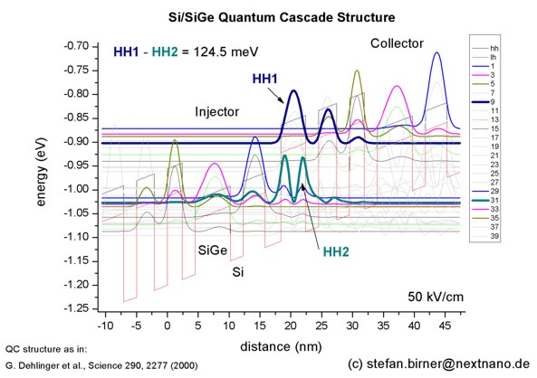
Figure 2.4.11.8 Calculated valance band edge (black line) of the quantum-cascade structure with electric field of strength 50 kV/cm applied. Also shown are the probability densities (\(\Psi^2\)) of several hole states, which are shifted by their corresponding eigenenergies.
Last update: nn/nn/nnnn