Parabolic Quantum Well (GaAs / AlAs)
- Input files:
parabola_half-parabola_nnpp.in
- Scope:
This tutorial aims to reproduce figures 3.11 and 3.12 (pp. 83-84) of [HarrisonQWWD2005], thus the following description is based on the explanations made therein.
General comments on the solutions of a parabolic potential
An ideal parabolic potential represents a “harmonic oscillator” which is described in nearly every beginner’s textbook on quantum mechanics. The eigenstates can be calculated analytically and are given by the following relationship:
where \(n\) = 1, 2, 3, …
One feature of a particle that is confined in such a well is that the energy levels are equally spaced by \(\hbar\omega_0\) above the zero point energy of 1/2 \(\hbar\omega_0\).
The eigenfunctions show an even-odd alternation which is also the case in symmetric, square quantum wells.
The eigenenergies can be measured experimentally by analyzing the optical transitions between the conduction and the valence band states, taking into account the selection rules (both states must have the same parity, see tutorial on interband transitions). For intersubband transitions, different selection rules apply (see tutorial on intersubband transitions). Such an experiment can be used to measure the conduction and valence band offsets because the curvature of the conduction and valence band edges (and thus the eigenstates) depends on the offsets.
More information on this can be found in [Davies1998].
Parabolic quantum well: 10 nm \(AlAs\) / 10 nm \(AlGaAs\) / 10 nm \(AlAs\)
It is possible to grow parabolic quantum wells by continuously varying the composition of an alloy. Our structure consists of a 10 nm \(Al_xGa_{1-x}As\) parabolic quantum well (the \(x\) alloy content varies parabolically) that is surrounded by 10 nm \(AlAs\) barriers on each side. We thus have the following layer sequence: 10 nm \(AlAs\) / 10 nm \(Al_Ga_{1-x}As\) / 10 nm \(AlAs\).
Bandeges
Figure 2.4.5.1 shows the conduction band edge and the three lowest electron wave functions (\(\psi\)) that are confined inside the parabolic quantum well. All other states are not confined anymore.
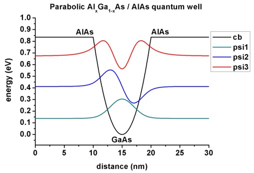
Figure 2.4.5.1 Calculated conduction band edge and the three lowest electron wave functions that are confined inside the parabolic QW. The energies were shifted so that the conduction band edge of \(GaAs\) equals 0 eV.
The figure is in perfect agreement with Fig. 3.11 (p. 83) of [HarrisonQWWD2005].
Technical details
The parabolic potential is specified by using a parabolic alloy profile.
structure{
    ...
    region{
        line{ x = [ -5.0 , 5.0 ] }
    }
    ternary_linear{
        name = "In(x)Ga(1-x)As"
        alloy_x = [0.0, 1.0]
        x = [ -5.0, 5.0]
    }
}
In agreement with Paul Harrison, we assumed a constant effective mass of 0.067 \(m_0\) throughout the whole sample and further assumed the conduction band offset between \(GaAs\) and \(AlAs\) to be 0.83549 eV.
Output
The conduction band edge of the Gamma conduction band can be found here bias_00000\bandedge_Gamma.dat. The 1st column contains the position in units of [nm] and the 2nd column contains the conduction band edge in units of [eV].
The file probabilities_shift_quantum_region_Gamma.dat contains the eigenenergies and the squared wave functions (\(Psi^2\)). The 1st column contains the position in units of [nm]. Note that the \(\Psi^2_n\) are shifted with respect to their energy \(E_n\) so that they can be nicely plotted into the conduction band profile.
amplitudes_shift_quantum_region_Gamma.dat contains the eigenenergies and the wave functions (\(Psi\)). The 1st column contains the position in units of [nm]. Note that Psin is shifted with respect to its energy En so that they can be nicely plotted into the conduction band profile.
Both probabilities_shift_quantum_region_Gamma.dat and amplitudes_shift_quantum_region_Gamma.dat contain the eigenenergies of the electron states in units of [eV]. Paul Harrison uses a 0.01 nm grid whereas we use the 0.01 nm grid only in the middle of the device (or 0.02 nm), but at the boundaries (i.e. from 0 nm to 5 nm and from 25 nm to 30 nm) we use a 0.1 nm grid to avoid long CPU times. The eigenvalues read:
\(n\) |
\(E_n\) (nextnano++) |
\(E_n\) ([HarrisonQWWD2005]) |
1 |
0.13777630889948 |
0.1377751623 |
2 |
0.41211073419019 |
0.4121058503 |
2 |
0.67581828697139 |
0.6755025905 |
Making use of equation (2.4.5.1) with \(\omega_0 = \sqrt{C/m^*}\) (\(m^*\) = effective mass, \(C\) = constant which is related to the parabolic potential \(V(x) = 1/2 Kx^2\)), one can calculate \(E_n\) = \(\hbar \omega_0\):
\(\hbar \omega_0\) = 2\(E_1\) - 0 eV = 0.276 eV
\(\hbar \omega_0\) = \(E_2\) - \(E_1\) = 0.274 eV
\(\hbar \omega_0\) = \(E_3\) - \(E_2\) = 0.264 eV
Obviously, due to the finite \(AlAs\) barrier that we have employed, the higher lying states deviate slightly from the analytical results where infinite barriers have been assumed.
Figure 2.4.5.2 shows the eigenenergies for the confined states \(E_1\), \(E_2\) and \(E_3\). As expected they are lying on a straight line because they are separated by \(\hbar\omega_0\). The figure is in perfect agreement with Fig. 3.12 (p. 84) of [HarrisonQWWD2005].
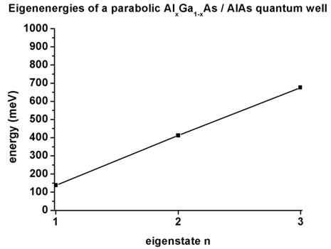
Figure 2.4.5.2 Eigenenergies for the three lowest states.
Matrix elements
The following matrix elements have been calculated:
interband_matrix_elements{}: This spatial overlap matrix elements \(\left\langle\psi_f|\psi_i\right\rangle\) simply returns the Kronecker delta as expected, because the wave functions are orthogonal.
intraband_matrix_elements{}: \(\left\langle\psi_f|p_x|\psi_i\right\rangle\) (see Tutorial on intraband transition)
dipole_moment_matrix_elements{}: \(\left\langle\psi_f|x|\psi_i\right\rangle\) (see Tutorial on intraband transition)
“Infinite” (30 eV) parabolic QW confinement for GaAs
Inputfile: 1DGaAs_ParabolicQW_infinite.in
Figure 2.4.5.3 shows the eigenstates of a parabolic quantum well (\(GaAs\)) where the confinement is assumed to be 30 eV. Now up to 37 eigenstates are confined in the quantum well (grid resolution: 0.025 nm inside the well, 0.05 nm inside the barrier).
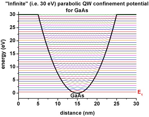
Figure 2.4.5.3 Calculated conduction band profile and probability densities (\(\Psi^2\)) for eigenstate \(n\) (\(n\) = 1, 2, …, 37).
Figure 2.4.5.4 shows the energies of the 37 confined electron states as a function of eigenstate \(n\). As expected, the curve shows a linear dependence because the eigenstates are equally spaced by \(\hbar\omega_0\) = 0.826 eV (where we used \(E_n\) = ( \(n\) - 1/2 ) \(\hbar\omega_0\)).
\(\hbar\omega_0\) = 2 \(E_1\) - 0 eV = 0.8261 eV |
\(E_1/(2 E_1)\) = 0.5000 |
\(\hbar\omega_0\) = \(E_2\) - \(E_1\) = 0.8260 eV |
\(E_2/(2 E_1)\) = 1.4999 |
\(\hbar\omega_0\) = \(E_3\) - \(E_2\) = 0.8260 eV |
\(E_2/(2 E_1)\) = 2.4997 |
\(\hbar\omega_0\) = \(E_4\) - \(E_3\) = 0.8259 eV |
\(E_4/(2 E_1)\) = 3.4994 |
\(\hbar\omega_0\) = \(E_5\) - \(E_4\) = 0.8259 eV |
\(E_5/(2 E_1)\) = 4.4991 |
\(\hbar\omega_0\) = \(E_6\) - \(E_5\) = 0.8258 eV |
\(E_6/(2 E_1)\) = 5.4987 |
\(\hbar\omega_0\) = \(E_7\) - \(E_6\) = 0.8258 eV |
\(E_7/(2 E_1)\) = 6.4982 |
\(\hbar\omega_0\) = \(E_8\) - \(E_7\) = 0.8257 eV |
\(E_8/(2 E_1)\) = 7.4978 |
Still, due to the “infinite” barrier of 30 eV (which is still a finite barrier) that we have employed, the higher lying states deviate slightly from the analytical results where infinite barriers have been assumed.
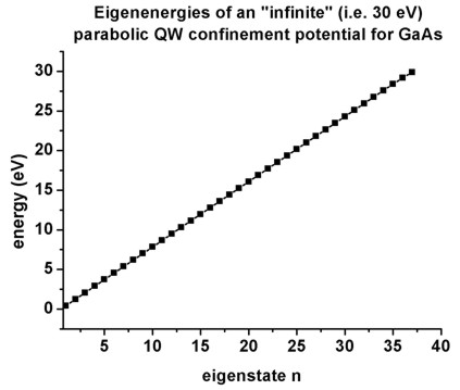
Figure 2.4.5.4 Eigenenergies of 37 eigenstates for an infinite parabolic QW.
One should bear in mind that the energy level spacing of such parabolic quantum wells is inversely proportional to both the well width and the square root of the effective mass.
It is also interesting to look at the intraband matrix elements, i.e. to investigate the probability for intersubband transitions. The relevant output is contained in these two files:
\bias_00000\Quantum\dipole_moment_matrix_elements_quantum_region_Gamma_100.txt - \(p_x\)
\bias_00000\Quantum\intraband_matrix_elements_quantum_region_Gamma_100.txt - \(x\)
From the calculated oscillator strengths it can be seen that only transitions from one level to the neighboring levels (+1 and -1) are allowed. Because in the case of a harmonic oscillator the momentum operator is proportional to the sum of the creation and the annihilation operators, thus only states can couple that have different occupation numbers with the difference equal to 1.
“Infinite” (30 eV) half-parabolic QW confinement for GaAs
Input file: 1DGaAs_ParabolicQW_infinite_half_nnpp.in
Figure 2.4.5.5 shows the eigenstates when taking only the right half of the parabolic quantum well (\(GaAs\)) that has been calculated above. The confinement is 30 eV on the right and infinite confinement on the left (Dirichlet boundary conditions). Now only 18 eigenstates are confined in the quantum well, i.e. half the number of the eigenvalues compared with the full parabolic QW (grid resolution: 0.025 nm inside the well, 0.05 nm inside the barrier). The figure shows the conduction band profile and the square of the wave functions (\(\Psi_n^2\)) for eigenstate \(n\) (\(n\) = 1, 2, …, 18).
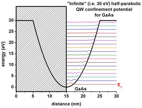
Figure 2.4.5.5 Calculated conduction band profile and probability densities (\(\Psi^2\)) for all confined eigenstates in an half-parabolic potential.
Again, the eigenstates are equally spaced. However, the separation energy is now twice as large as before, i.e. \(\hbar\omega_0\) = 2 \(\cdot\) 0.826 eV = 1.65 eV.
The ground state energy this time is given by: \(E_1\) = 3/2 \(\hbar\omega_0\)/2.
\(\hbar\omega_0\) = 4/3 \(E_1\) - 0 eV = 1.639 eV
\(\hbar\omega_0\) = \(E_2\) - \(E_1\) = 1.647 eV
\(\hbar\omega_0\) = \(E_3\) - \(E_2\) = 1.648 eV
\(\hbar\omega_0\) = \(E_4\) - \(E_3\) = 1.648 eV
It is also interesting to look at the intraband matrix elements, i.e. to investigate the probability for intersubband transitions. The relevant output is contained in these two files:
\bias_00000\Quantum\dipole_moment_matrix_elements_quantum_region_Gamma_100.txt - \(p_x\)
\bias_00000\Quantum\intraband_matrix_elements_quantum_region_Gamma_100.txt - \(x\)
Conclusion
We note that also more realistic parabolic quantum wells can be calculated with nextnano++. Assuming that the alloy profile is parabolic,
strain can be included (the strain tensor depends on the alloy profile),
as well as effective masses that depend on the alloy profile,
an 8-band k.p model (necessary to get correct intersubband transition energies)
and bowing parameters (especially important for \(AlGaAs\)).
All these features are automatically included in the nextnano++ code.
Last update: nn/nn/nnnn