Electron Flying Qubit
- Input Files:
EPJQT2022_2D_TCW_nnp.in
EPJQT2022_2D_ABI_nnp.in
EPJQT2022_1D_slice_TCW_nnp.in
In this tutorial, we discuss multi-terminal electron transport in various nanodevices. As an example, we focus on so-called electron flying qubits, which are solid-state counterparts of the quantum optics devices. Basic building blocks of these qubits are the following semiconductor-based nanodevices:
Tunneling-coupled wires, TCW - the electronic counterpart of the optical beam splitter, see Figure 2.4.14.14;
Aharonov-Bohm interferometer, ABI - the electronic counterpart of the optical interferometer, see the central region of Figure 2.4.14.15;
Circuits containing these elements connected in a series, see Figure 2.4.14.15.
Left rectangular regions in Figure 2.4.14.14 and Figure 2.4.14.15 (with numbers 1 and 2) are incoming leads, where the electron can be injected into the nanodevice. We will assume that it is injected into the lead 1. Right rectangular regions (with numbers 3 and 4) are outgoing leads, where the electron can be detected after propagating through the entire nanodevice. The functionality of the electron flying qubits requires a reflection-free propagation of the electron. If the electron is reflected and returns to one of the incoming leads, a part of the quantum information is lost. The important task of numerical simulations is to identify regimes where reflection is reduced as much as possible.
The interior part of the nanodevices is assumed to be made from 2D GaAs-based semiconductor and includes regions with different electrostatic potentials and applied gate voltages that govern the energy profile through which the electron propagates. Colors in Figure 2.4.14.14 and Figure 2.4.14.15 reflect the strength of the electrostatic potential in different parts of the device, ranging from \(0\) eV (dark blue color) up to \(\gg 1\) eV (dark red color). All building blocks of the electron flying qubit can be realized in experiments with the help of properly tuned gated regions.
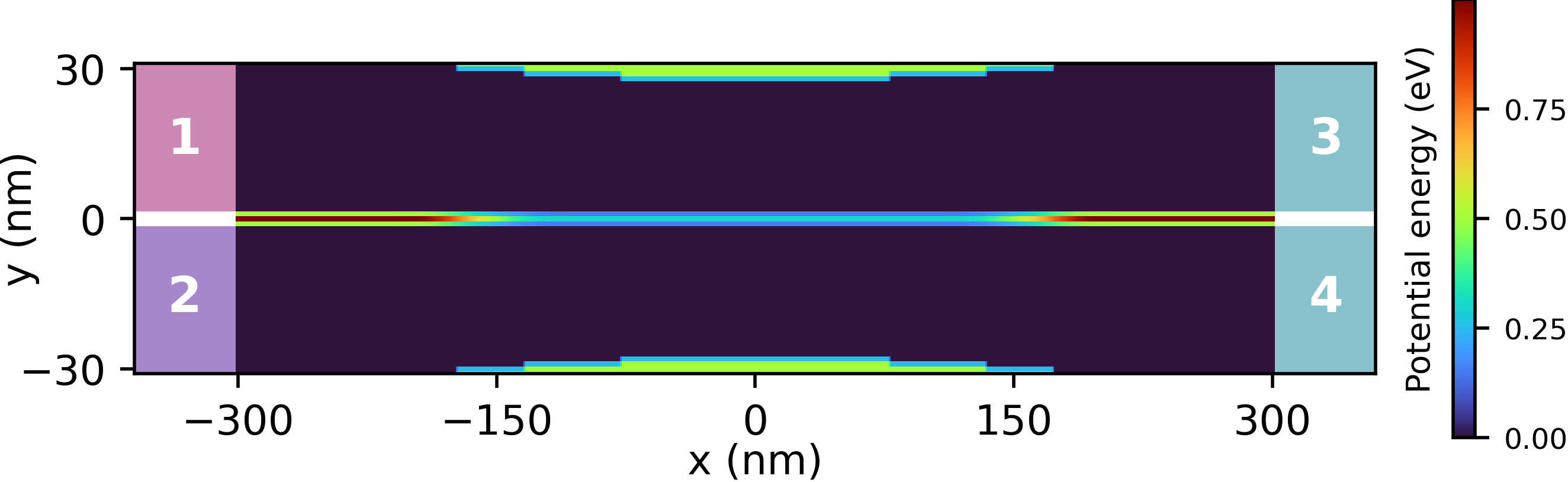
Figure 2.4.14.14 Geometry and potential landscape of TCW connected to four terminals (external leads marked by white numbers). Red and light blue separation regions denote impenetrable (very high with the height \(V_\infty\) = 10 eV) and penetrable (tunneling with the height \(V_T\) ) potential barriers, respectively. Green regions mark those parts of the device where the gate voltages 0.5 eV and \(V_g\) are applied.
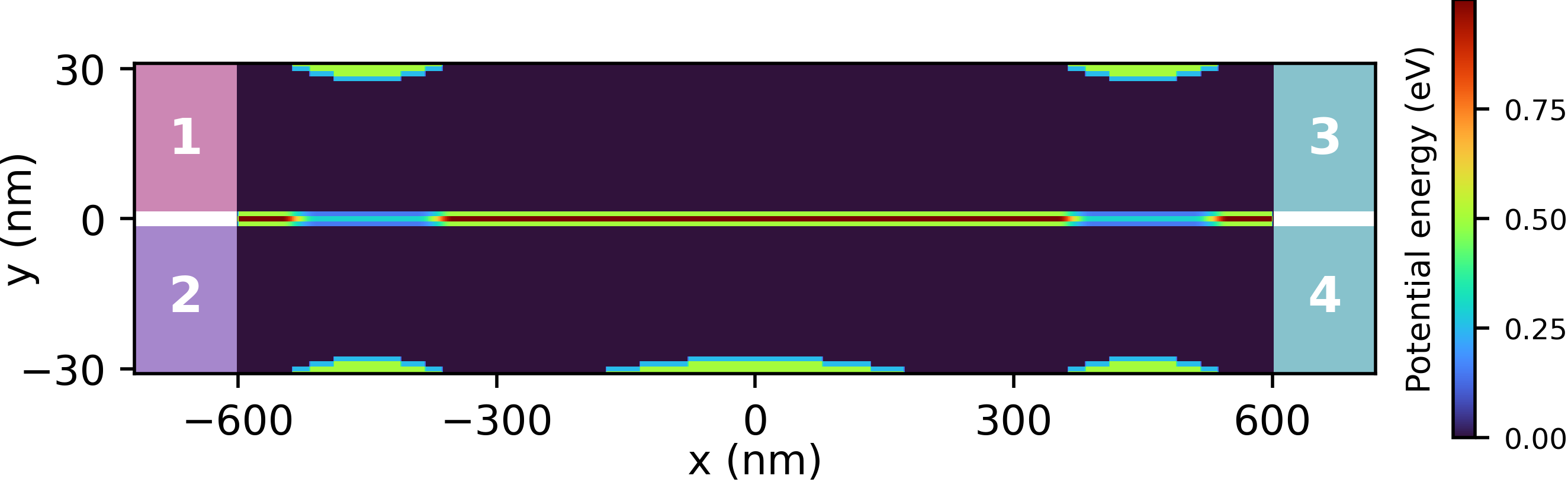
Figure 2.4.14.15 Geometry and potential of a circuit containing two TCWs and one ABI, also connected to four terminals. The additional barrier around x=0 in the lower path yields the electrostatic Aharonov-Bohm effect.
Let us first discuss transport in TCW. The horizontal line in Figure 2.4.14.14 shows a potential barrier separating two paths, along which the electron can move towards the outgoing leads. Red parts of the barrier are impenetrable for the electron while the electron can tunnel through the light blue segment. The latter is precisely the region where the quantum interference between the upper and lower paths takes place. Having experienced the interference, the electron wave function is split between the separated upper and lower paths. As a result, there is some probability to detect the electron in the outgoing leads 3 or 4, which depends both on the electron energy and on the parameters of the nanodevice, including the height of the tunneling barrier.
The TCW-ABI-TCW device shown in Figure 2.4.14.15 consists of two TCW (left and right outer) regions and the electrostatically induced ABI (central) region. In addition to the interference in the TCWs, the interference is influenced by the asymmetric gating in ABI: The electron trajectories traversing the lower and upper paths in ABI, which are separated by the impenetrable potential barrier, require different geometric phases governed by this asymmetric gating. This phase changes the interference and the transmmition through the entire device.
The nextnano software allows one to calculate the partial local density of states, Figure 2.4.14.16, and the transmission from the lead 1 to the leads 3 and 4, Figure 2.4.14.17 and Figure 2.4.14.18, in both, TCW and TCW-ABI-TCW, devices. The theoretical background involves the numerical solution of the Schrödinger equation by using the Contact Block Reduction method.
The partial local density of states, pLDoS, represents the probability of finding the propagating electron (that was injected with an energy E at the lead 1) at a certain position. The coordinate dependence of pLDoS illustrates how the electron with a given energy propagates through the device. The energy dependent transmission, \(T_{ij}(E)\), is determined by the probability for the electron which is injected into lead i to reach lead j. Readers can find more information on these quantities in one of standard textbooks.
nextnano GmbH simulations of the pLDoS and of the transmission are discussed in detail our recent review (see SpringerOpen or ArXiv) which presents the progress of the EU Ultrafastnano project. Let us emphasize here that these simulations are valuable tools to identify the parameter range where the reflection of the propagating electron, either to the lead no. 1 or to the lead no. 2, is minimized and, simultaneously, there is a pronounced manifestation of the quantum interference. Hence, one can find an optimal basic configuration for the realization of the electron flying qubit. Such a preliminary optimization saves a lot of experimental efforts and can substantially accelerate the overall progress.
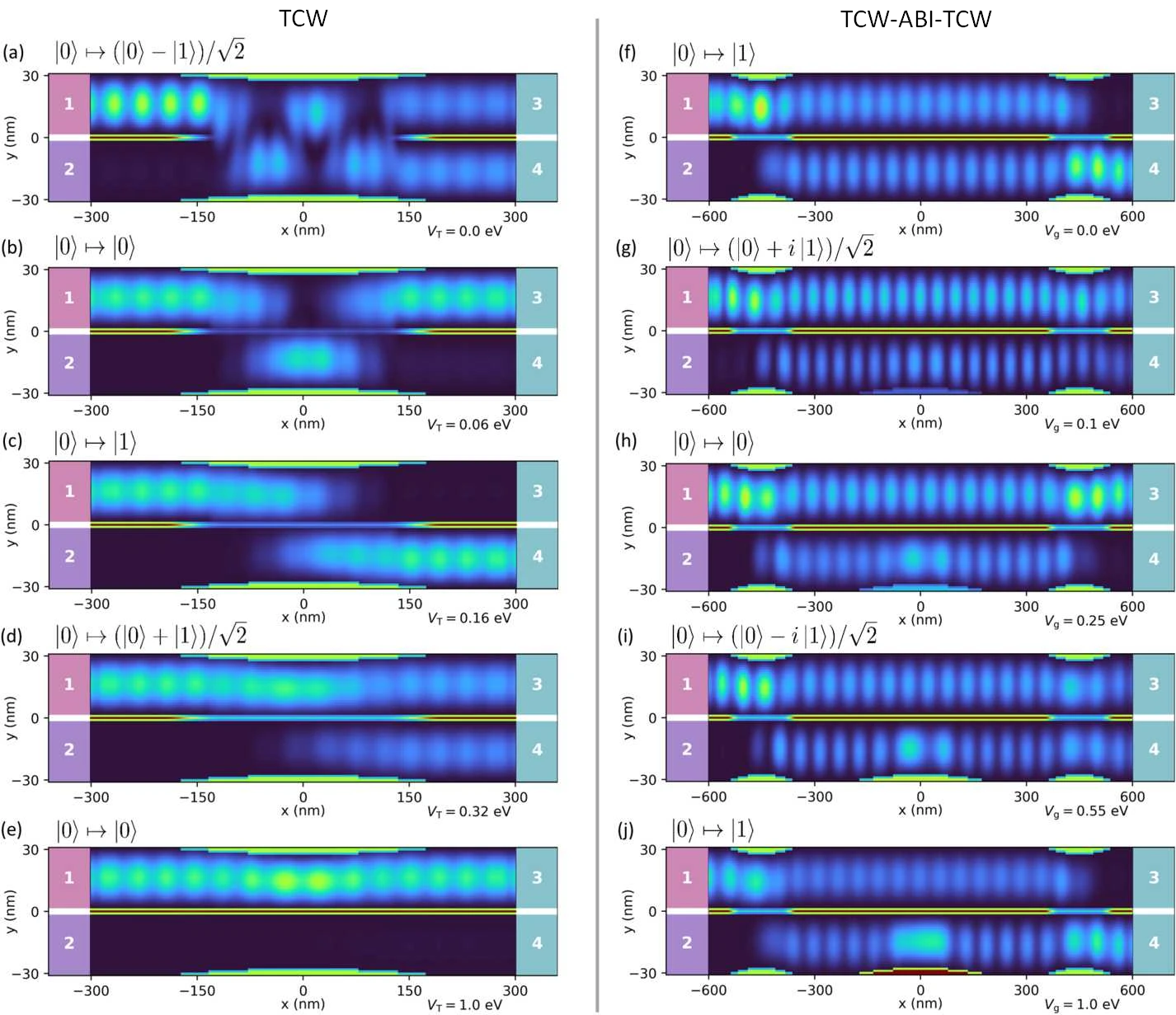
Figure 2.4.14.16 nextnano GmbH simulations of the electron partial local density of states in TCW [panels (a-e)] and the TCW - ABI - TCW [panels (f-j)] nanodevices. Both devices are connected to four terminals (marked by white numbers). The background shows the potential landscape defined by the voltage on the surface gates. The electron with a given energy (E = 9.2 meV for TCW and E = 7.5 meV for TCW-ABI-TCW) is always injected into the upper incoming channel from lead 1. The states at the output leads are indicated at the top of each plot, with the 0 and 1 qubit states corresponding to the densities at output leads 3 and 4. Panels (a-e): the pLDoS in TCW for increasing the tunneling barrier voltage (described by \(V_T\) ). Panels (f-j): the pLDoS in TCW-ABI-TCW for increasing voltage on a side gate of the bottom path (described by \(V_g\)).
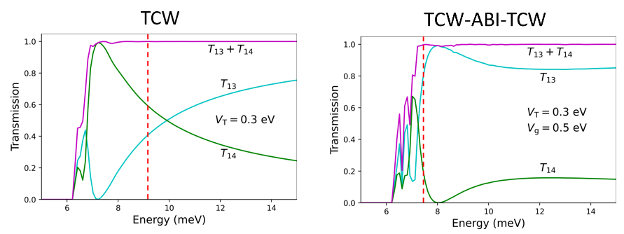
Figure 2.4.14.17 Energy-dependent transmission of the electron from the lead no. 1 into the leads no. 3 (\(T_{13}\) ) and no. 4 (\(T_{14}\)). Red dashed lines mark some electron energies where the reflection is almost absent, \(T_{13}\) + \(T_{14}\) \(\simeq\) 1 (E = 9.2 meV for TCW and 7.5 meV for TCW-ABI-TCW).
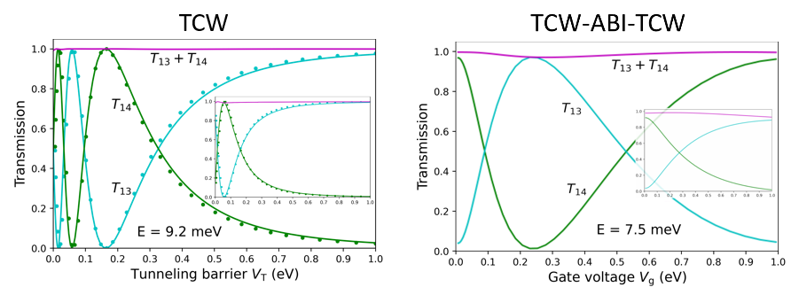
Figure 2.4.14.18 Almost reflectionless transmission of the electron with fixed energy as a function of \(V_T\) (TCW) and \(V_g\) (TCW-ABI-TCW). Dots in the left panel correspond to the semi-phenomenological theory supplied by the 1D simulation of the spectrum at the center of the device, x = 0. Insets: The same dependence as in the main figures but for devices with half-length, where the accessible number of quantum oscillations is much smaller.
To conclude we note that this tutorial exemplifies the simulations done for a simple toy-model describing physics of the nanodevices. Nevertheless, the nextnano software can be used to simulate more realistic geometries whose potential profile can be obtained from electrostatic simulations. The restriction to 2D GaAs-based semiconductor materials is also not crucial, since input files can be easily adapted, e.g., for Si-based ones.
- Acknowledgment
This tutorial is based on the nextnano GmbH collaboration in the scope of the UltraFastNano Project aiming at development of the first Flying Electron Qubit at the picosecond scale, and it is funded by the European Union’s Horizon 2020 research and innovation program under grant agreement No 862683.
Last update: nn/nn/nnnn