Ultrathin-body Double Gate Metal Oxide Semiconductor Field Effect Transistor (DG MOSFET) (5 nm)
Attention
This tutorial is under construction
- Input files:
DG-MOSFET-5nm_Si_Birner_APPA_2006_2D_cl_nnp.in
DG-MOSFET-5nm_Si_Birner_APPA_2006_2D_qm_nnp.in
- Scope:
This tutorial compares classical and quantum mechanical simulations of a Double Gate MOSFET (DG MOSFET). This tutorial is related to the following publication: [BirnerAPhys2006].
- Output files:
bias_xxxxx\density_electron.dat
bias_xxxxx\bandeges.dat
IV_characteristics.dat
Structure
The main idea of a Double Gate MOSFET is to control the Si channel very efficiently by choosing the Si channel width to be very small and by applying a gate contact to both sides of the channel. This concept helps to suppress short channel effects and leads to higher currents as compared with a MOSFET having only one gate. The structure in this tutorial consists of an intrinsic Si channel having the length 25 nm and the width 5 nm, as shown in Figure 2.5.1.69. The channel is connected to heavily n-type doped source and drain regions of length 10 nm each (constant doping profile with a concentration of \(1\cdot 10^{20}\,\mathrm{cm^{-3}}\), fully ionized). The gates have a length of 25 nm and are separated from the Si channel by a 1.5 nm thick \(\mathrm{SiO}_2\) layer with static dielectric constant \(\epsilon = 3.9\).
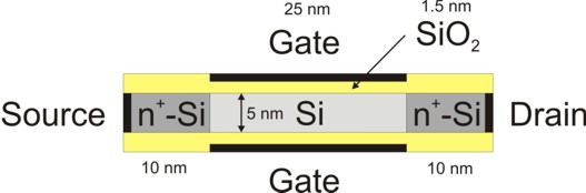
Figure 2.5.1.69 Geometry of the DG MOSFET, which consists of source contact, n-type doped source region (Si), Si channel (undoped), n-type doped drain region (Si), drain contact, \(\mathrm{SiO}_2\) insulator, top gate and bottom gate.
In the simulations, a grid spacing of 1 nm and 0.5 nm are chosen for the \(x\)- and \(y\)-direction, respectively.
We apply a voltage of \(V_\mathrm{SD} = 0.5\,\mathrm{V}\) to the drain contact. The gate voltage is varied from -0.3 V to 1.0 V in steps of 0.1 V. At the gate a Schottky barrier of 3.075 eV is chosen to mimic the gate electrode work function which has been assumed to be 4.1 eV.
For the mobility we employ the arora mobility model. In this model, the mobility is assumed to depend on temperature (\(T = 300\,\mathrm{K}\)) and on the ionized dopants (\(N_\mathrm{D}\)), but is independent of the electric field. Thus, we have two different electron mobilities:
n-type doped Si region: \(64.47\,\mathrm{cm^2/Vs}\)
intrinsic Si region: \(1429.2\,\mathrm{cm^2/Vs}\)
Electron density and conduction band profile
Figure 2.5.1.70 shows a slice through the middle of the device along the \(y\)-direction, i.e. through the gate contacts. The source drain voltage is \(V_\mathrm{SD} = 0.5\,\mathrm{V}\), and the gate voltage is \(V_\mathrm{G} = 0.7\,\mathrm{V}\). Two results are shown:
classical calculation with self-consistent solution of the two-dimensional Poisson and current equations. Here, the current equation is solved within a drift-diffusion model based on the classical density. For the classical calculation the input file DG-MOSFET-5nm_Si_Birner_APPA_2006_2D_cl_nnp.in should be used.
quantum mechanical calculation with self-consistent solution of the two-dimensional Poisson, Schrödinger and current equations. Here, the current equation is solved within a drift-diffusion model based on the quantum mechanical density. For the quantum mechanical calculation the input file DG-MOSFET-5nm_Si_Birner_APPA_2006_2D_qm_nnp.in should be used.
The Fermi level is almost flat, i.e. constant (-0.249 eV) and very similar in both simulations. The conduction band edge in the Si channel is lower in the case of the quantum mechanical simulation. The main difference can be attributed to the electron density. The classical density has its maximum at the \(\mathrm{Si/SiO}_2\) interface, because \(E_\mathrm{F,n} - E_\mathrm{C}\) has its maximum there. The quantum mechanical density is practically zero at the \(\mathrm{Si/SiO}_2\) interface, because the wave functions tend to zero due to the \(\mathrm{SiO}_2\) barrier. One can clearly see that the electron density has the highest values in the middle of the channel and not at the \(\mathrm{Si/SiO}_2\) interfaces.
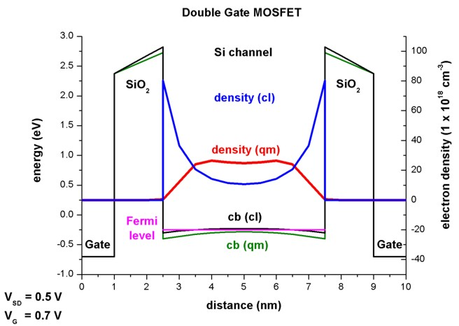
Figure 2.5.1.70 Conduction band profile, electron density and Fermi energy across the DB MOSFET structure at gate voltage \(V_\mathrm{G} = 0.7\,\mathrm{V}\).
Figure 2.5.1.71 and Figure 2.5.1.72 show the conduction band edge, charge densities and Fermi levels at the voltage of \(V_\mathrm{G} = 0.3\,\mathrm{V}\) (closed channel) and \(V_\mathrm{G} = 1.0\,\mathrm{V}\) (open channel), respectively. The quantum mechanical density has different shapes at different voltages (one maximum in the middle vs. two maxima off-the-center). Note that the axes for the electron density are scaled differently.
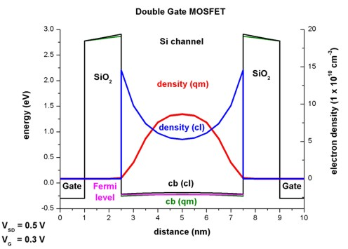
Figure 2.5.1.71 Conduction band profile, electron density and Fermi energy across the DB MOSFET structure at gate voltage \(V_\mathrm{G} = 0.3\,\mathrm{V}\).
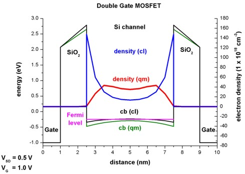
Figure 2.5.1.72 Conduction band profile, electron density and Fermi energy across the DB MOSFET structure at gate voltage \(V_\mathrm{G} = 1\,\mathrm{V}\).
Electron wave functions
In our simulations we only consider electron states from the Delta{} conduction band. There are three Schrödinger equations that have to be solved each time having the following mass tensors that enter the Hamiltonian \(H(x, y)\):
with \(m_\mathrm{longitudinal} = 0.916\,m_0\) and \(m_\mathrm{transversal} = 0.190\, m_0\). Note that \(m_{zz}(x,y)\) does not enter the Hamiltonian, but \(m_{zz}(x,y)\) is used to calculate the quantum mechanical density (\(k_\parallel\) dispersion). The quantum mechanical density for such a two-dimensional simulation is proportional to the square root of \(m_{zz}(x,y)\). More precisely, the quantum mechanical density is obtained for each grid point by evaluating
which implies:
summation over all eigenstates \(i\)
evaluation of the square of the wave function \(\big|\psi_i(x,y)\big|^2\)
weighting \(\big|\psi_i(x,y)\big|^2\) with the Fermi-Dirac integral \(\mathcal{F}_{-1/2}\big[ (E_\mathrm{F} - E_i) / k_\mathrm{B}T \big]\), which includes the \(\Gamma(1/2)\) pre-factor of the Fermi-Dirac integral
multiplication by a factor which includes the square root of \(m_{xx} k_\mathrm{B}T / (2 \pi \hbar^2)\) and the spin and valley degeneracy \(g_\mathrm{spin, valley}\).
Most of the wave functions are located in the source and drain region. In Figure 2.5.1.73 and Figure 2.5.1.74, the lowest wave functions \(\psi^2\), which contribute to the quantum mechanical charge density in the region where the 1D slice was taken (i.e. in the middle of the device (\(V_\mathrm{G} = 0.7\,\mathrm{V}\), \(V_\mathrm{SD} = 0.5\,\mathrm{V}\))), are shown. The Fermi energy along the 1D slice through the middle of the device lies at -0.249 eV. The states are labelled from top to bottom: (Note: They are sorted by energies, but their distance is not equivalent to their energy spacing.)
deg1: \(35^\mathrm{th}\) state with \(E_{35} = -0.215\,\mathrm{eV}\) (\(\psi^2\) is zero at the 1D slice which can be seen in Figure 2.5.1.74)
deg1: \(32^\mathrm{nd}\) state with \(E_{32} = -0.224\,\mathrm{eV}\) (25 meV above Fermi level)
deg3: \(13^\mathrm{th}\) state with \(E_{13} = -0.226\,\mathrm{eV}\) (23 meV above Fermi level)
deg2: \(32^\mathrm{nd}\) state with \(E_{32} = -0.250\,\mathrm{eV}\) (below Fermi level, corresponding to \(2^\mathrm{nd}\) subband)
deg2: \(25^\mathrm{th}\) state with \(E_{25} = -0.277\,\mathrm{eV}\) (below Fermi level, corresponding to \(1^\mathrm{st}\) subband)
Here, deg1 are the states originating from the valleys having the light, transversal mass perpendicular to the channel (i.e. these states have higher energies), deg3 are the states originating from the valleys having the light, transversal mass in the plane of the channel \(m_{xx} = m_{yy} = m_\mathrm{transversal} = 0.190 m_0\) (high energies due to light masses) and deg2 are the states originating from the valleys having the heavy, longitudinal mass perpendicular to the channel as is the case in standard MOSFETs (i.e. these are the states that are occupied because the energies are the lowest).
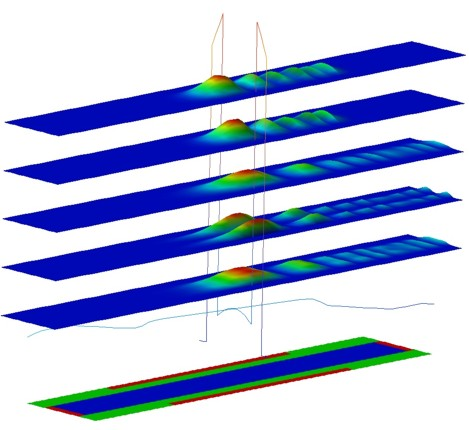
Figure 2.5.1.73 Wavefunctions located inside the Si-channel for \(V_\mathrm{G} = 0.7\,\mathrm{V}\) and \(V_\mathrm{SD} = 0.5\,\mathrm{V}\).
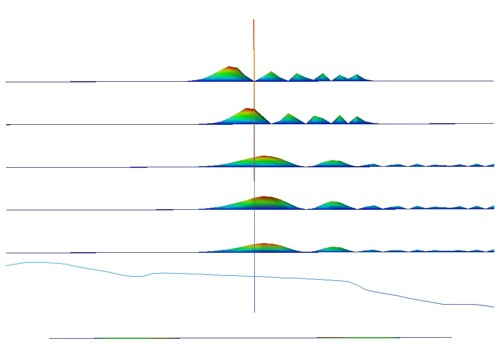
Figure 2.5.1.74 Wavefunctions located inside the Si-channel for \(V_\mathrm{G} = 0.7\,\mathrm{V}\) and \(V_\mathrm{SD} = 0.5\,\mathrm{V}\) (side-view).
I-V characteristics
The current-voltage (I-V) characteristic can be found in the following file: IV_characteristics.dat. The drain voltage has been kept constant at 0.5 V and the gate voltage varied from -0.3 V to 1.0 V. The resulting I-V curve is plotted in Figure 2.5.1.75. Due to the influence of quantum mechanics the current densities obtained from the quantum mechanical calculations are lower than from the classical calculations.
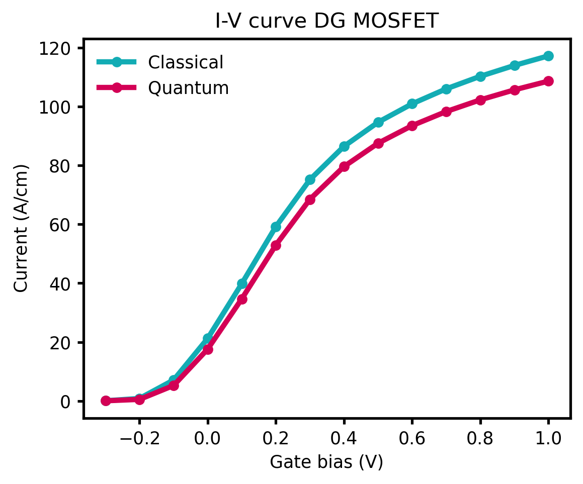
Figure 2.5.1.75 Comparison between classical and quantum mechanical calculation of the I-V characteristics.
Note that the absolute magnitude of the current is determined mostly by the mobility model. By using a more realistic mobility model that takes into account the dependency of the parallel and perpendicular electric fields, a smaller current would be obtained.
Last update: nn/nn/nnnn