Maximizing Envelope Overlaps for a Given Transition Energy
Attention
The nextnanoevo Python package is under development. Its release is planned for 2024.
Header
- Relevant files
T2SL_InAs-GaInSb_Grein_JAP_1995_1D_nnp.in (the same as here)
InGaSb_InAs_script.py (not available yet)
- Scope
design optimization
envelope overlaps
transition energies
type-II superlattice
- Important variables
$L_InGaSb = thickness of the layer of In(x)Ga(1-x)Sb (nm)
$L_InAs = thickness of the layer of InAs (nm)
$X_InGaSb = indium content of the layer of In(x)Ga(1-x)Sb
\(E_0\) = fundamental transition energy
\(S\) = overlap between the c1 and v1 wave function envelopes
\(d\) = fitness (distance from the ideal solution)
Introduction
This tutorial briefly introduces concept of evolution strategies for semiconductor device optimization and discusses its application on an example of type-II superlattice from a tutorial 1D - InAs/In0.4Ga0.6Sb superlattice dispersion with 8-band k.p (type-II band alignment) using nextnanoevo package.
Evolutionary algorithms
Evolutionary algorithms are algorithms inspired by biological processes such as selection, mutation and reproduction that are used to solve optimization problems. In this tutorial, we specifically use the so-called NSGA-II genetic algorithm (see more details below) to improve the design of a type-II superlattice semiconductor device. The objective is to obtain a fundamental transition energy of 0.15 eV and to maximize the envelope overlaps between of the first conduction band c1 and the first valence band v1 states. The algorithm begins with a template design and a set of initial parameters to be modified as well as ranges within which the parameters can be adjusted. The ranges of these parameters form the search space for the algorithm and should highly depend on experimental feasibility.
The template ‘default’ design constitutes the initial parent population. From this first generation, a few modifications (mutations) of the initial design are made to generate a new set of designs which forms the children population. Then, nextnano++ is used to evaluate the fitness of each individual of this new population. The fitness function is defined based on the optimization objectives chosen by the user. The best individuals are selected according the fitness function and become the next parent population to then have children of their own. Again, the best designs are selected to repeat the process of mutation, reproduction, and selection over and over again until the optimal design is reached. The algorithm stops when the objectives have been reached or, in the case of more loosely-defined objectives (i.e. maximize the overlap), the user sets the number of iterations (or generations) before starting the algorithm.
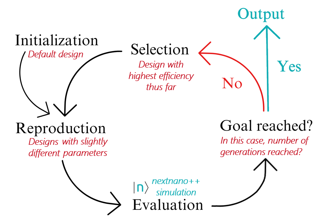
Figure 7.3.1 Diagram of the evolutionary algorithm combined with nextnano++.
Algorithm NSGA-II
There are several evolutionary algorithms that can be used to solve multi-objective problems but in this tutorial, NSGA-II (non-dominated sorting genetic algorithm) as developed by PyGMO was employed (for more information, visit the PyGMO documentation page). NSGA-II is a genetic algorithm that employs techniques such as non-dominated sorting and crowding distance to solve problems in a way that promotes elitism and diversity.
Non-dominated sorting is a technique used in multi-objective problems to identify the solutions that cannot be improved in any objective without worsening another objective, which can also be referred to as the Pareto-optimal solutions.
Crowding distance is a measure of how close a solution is to its neighbors. Solutions with a large distance to their neighbors are more likely to be selected for the next step in the algorithm than solutions with a small crowding distance to ensure the well-representation of the Pareto front in the next generation of solutions.
There are different parameters for the evolution process which can be tuned by the user, the most important one being the number of generations. The bigger it is, the longer the simulation will take but the better the results will possibly be. However, it is possible to reach the best result just after a couple of generation. For example, in this tutorial, the number of generations is set to 100, but the best design is obtained at the 50th generation. Or for example, one could also tune the crossover and mutation probabilities, that is the likelihood of two individuals combining their “genes” and the likelihood of a random change in an individual, respectively.
Parameters for optimization algorithm:
Variable |
Value |
Description |
|---|---|---|
alg |
‘nsga2’ |
name of the algorithm |
gen |
[100] |
number of generations - int or list of int |
cr |
0.95 |
crossover probability - float, [0,1[ |
eta_c |
10 |
distribution index for sbx crossover - float, [0,100[ |
m |
0.01 |
mutation probability - float, [0,1[ |
eta_m |
50 |
distribution index for polynomial mutation - float, [0,100[ |
seed |
876624 |
seed for randomness - int |
Note
Note: the evolution process is random, so each run may give a different result. Our suggestion is to change the seed (input a random number) for every run to promote randomness.
How to run the optimization
Requirements:
Install the nextnanoevo module (see instructions here)
download Python scripts nextnanoevo.py and InGaSb_InAs_script.py
download nextnano++ input file T2SL_InAs-GaInSb_Grein_JAP_1995_1D_nnp.in
Steps to follow:
Create a main folder containing the two Python scripts nextnanoevo.py and InGaSb_InAs_script.py and the nextnano input file InAs_InGaSb.in as well as an “output” folder.
Open InGaSb_InAs_script.py and copy the path to the InAs_InGaSb.in input file as well as the path to the output folder.
OPTIONAL: tune the parameters of the optimization such as the lower and upper boundaries of the parameters to optimize, the parameters of the default design or the number of generations.
Execute the script to run the optimization.
At the end of the run, the parameters and properties of the optimized design will be printed. This information will also be saved in a data file along with all the designs that have been simulated throughout the run. The data file can be found in the output folder, under “results”. The simulation results of both the default and optimized designs are also saved in the output folder and are named in the following way: [filename]_[L_InGaSb]_[L_InAs]_[X_InGaSb]. For example, the results of the default design will be the following folder: T2SL_InAs-GaInSb_Grein_JAP_1995_1D_nnp_1.5_3.98_0.4.
Optimizing type-II superlattice
Defining optimization problem
Let’s define optimal structure as the one characterized by a fundamental transition energy of 0.15 eV with the envelope overlaps between of the first conduction band c1 and the first valence band v1 states equal 1.
To run an evolution with nextnanoevo, a default design is provided by the user as well as parameters to optimize along with a search space, that is to say both lower and upper limits for each of these parameters.
For this device, the parameters to optimize were the thicknesses of the two layers of InGaSb and InAs as well as the indium content of the InGaSb layer. Our default design had the following parameters and properties:
Variable |
Value |
Description |
|---|---|---|
$L_InGaSb |
1.5 nm |
Thickness of the layer of In(x)Ga(1-x)Sb |
$L_InAs |
3.98 nm |
Thickness of the layer of InAs |
$X_InGaSb |
0.4 |
Indium content of the layer of In(x)Ga(1-x)Sb |
\(E_0\) |
0.10 eV |
Fundamental transition energy |
\(S\) |
0.497 |
Overlap between the c1 and v1 wave function envelopes |
\(d\) |
0.677 |
Fitness of the solution / distance from the ideal solution |

Figure 7.3.2 Band edges and energy levels (a) and energy dispersion of conduction, heavy hole and light hole bands along two directions in (\(k_x,k_y\)) space (b) of the default design.
And the defined search space was:
Variable |
Value |
|---|---|
$L_InGaSb |
[0.1, 10] nm |
$L_InAs |
[0.1, 10] nm |
$X_InGaSb |
[0.01, 1] |
To assess the performance of our candidate designs, we calculated the fundamental transition energy:
and the overlap between the c1 and v1 wave function envelopes:
Then, the fitness of a candidate is calculated by its distance from the ideal solution, that is the solution with the desired energy and overlap (in our case 0.15 eV and 1, respectively):
During the optimization process, this distance should decrease as we reach our optimized design which is the closest to the ideal solution.
Optimized design
At the end of our optimization run, the best design we obtained had the following parameters and properties:
Variable |
Value |
Description |
|---|---|---|
$L_InGaSb |
1.47 nm |
Thickness of the layer of In(x)Ga(1-x)Sb |
$L_InAs |
1.98 nm |
Thickness of the layer of InAs |
$X_InGaSb |
0.75 |
Indium content of the layer of In(x)Ga(1-x)Sb |
\(E_0\) |
0.152 eV |
Fundamental transition energy |
\(S\) |
0.723 |
Overlap between the c1 and v1 wave function envelopes |
\(d\) |
0.277 |
Fitness of the solution / distance from the ideal solution |

Figure 7.3.3 Band edges and energy levels (a) and energy dispersion of conduction, heavy hole and light hole bands along two directions in (\(k_x,k_y\)) space (b) of the optimized design.
Conclusion
We successfully obtained a design with the desired fundamental transition energy of 0.15 eV showing promise for applications in long-wave infrared detectors. The overlap of the wave function envelopes was also increased thus improving the overall performance of the device. The overall fitness of the design went from 0.677 to 0.277 by changing the lengths of the two layers by a few nanometers as well as the indium content in the InGaSb layer. This solution was the one that yielded the best trade-off between the objective transition energy and the highest overlap possible. However, other solutions in the Pareto front showed higher overlap values but slightly different transition energies than the objective or transition energies closer to the objective but lower overlap values.