This is the tool where we put on most effort in improving it by adding new features.
The nextnano³ tool is mainly distributed for historical reasons.
The nextnano³ tool is written in Fortran.
It has been developed at the Walter Schottky Institute from 1999 to 2010.
The nextnano++ tool is written in C++.
It has been developed at the Walter Schottky Institute from 2004 to 2008.
The tools have been written by different people that were working
at the Walter Schottky Institute of the Technische Universität München
in the Theoretical Semiconductor Physics group of Prof. Peter Vogl.
Essentially, both tools cover the same physics and methods, namely
treat the magnetic field within the \(\mathbf{k} \cdot \mathbf{p}\) approach
calculate the g tensor
include quaternary materials.
The nextnano++ tool is much faster for drift-diffusion calculations and for 2D/3D simulations.
For instance, if you work on LEDs, MOSFETs or Quantum Dots, nextnano++ is much better suited.
There are some applications where it is irrelevant which tool to use.
In this case we recommend to use both.
This has the advantage that the results of one tool can be compared to the results of the other one in order to gain more confidence in them.
For some applications, one tool should be preferred.
Please contact <support[at]nextnano.com> to find out which tool to choose for your particular application.
‘’$’’ character for the variables: $QuantumWellWidth=5.0`
‘’#’’ character for comments: #Thisisacomment. (# is also supported by nextnano³.)
Can I convert nextnano³ input files into nextnano++ input files?
Within nextnanomat, there is an experimental feature to convert a nextnano³ input file to a nextnano++ input file.
How to use this automatic conversion:
In the menu select
Tools==>Convertnextnano³inputfiletonextnano++
When you use the automatic conversion of nextnano³ input file into nextnano++,
you will find that it probably does not work completely.
If you save and run the nextnano++ input file that has been converted and that has the suffix _nnp.in,
very likely some errors appear indicating which line(s) to change.
Then some manual adjustments are needed, but the rough structure should help a lot for the conversion.
How can I track how much memory is used during the simulations?
Can I pass additional command line arguments to the executable?
Yes, this is possible. Go to
Tools ==> Options ==> Expertsettings ==> Commandline
For nextnano³, one could use for instance:
-database"D:\Myfolder\nextnano3\Syntax\my_database_nn3.in
-threads4
How can I speed up my calculations with respect to CPU time?
The most obvious way is to reduce the number of grid points you are using.
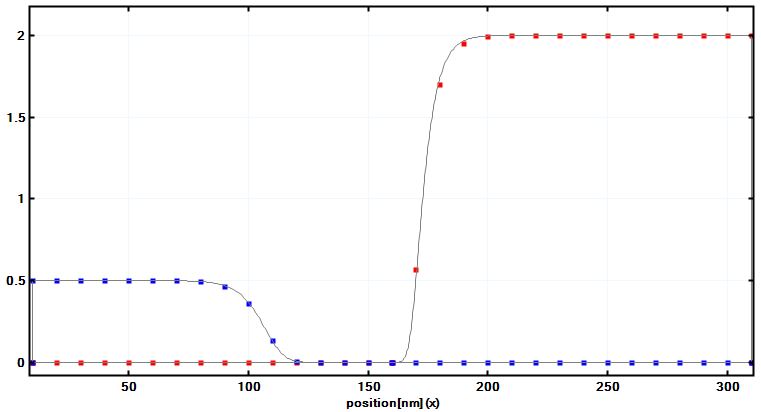
For instance, for the following p-n junction simulation,
a grid spacing of 1 nm was used (gray lines in Figure 10 ).
If one is using a coarse grid of only 10 nm, the calculated values (squares in Figure 10)
agree very well with the calculated values of the thin lines.
Figure 10 Hole (blue) and electron (red) densities of the p-n junction in units of \(10^{18} cm^{-3}\).
The gray lines are from simulations using a 1 nm grid spacing.
The squares are from a simulation that uses only a 10 nm grid resolution.
Note that the center coordinate of this plot is x=160 nm.
The depletion width for the holes is around wp:math:approx`50 nm,
for the electrons it is wn:math:approx`10 nm which is of the order of the grid spacing.
Even in this case, the calculated electron density is reasonably accurate.
The difference in CPU time comes from the fact that for the 10 nm resolution
the dimension of the matrix that is used for discretizing the Poisson equation is 30,
while in the case for the 1 nm grid spacing it has the dimension 300.
The proper choice of an optimal grid spacing is very relevant for 2D and 3D simulations,
as can be seen in the following.
1D simulation (length of sample: x = 300 nm)
1 nm grid spacing: dimension of Poisson matrix: \(N=300\)
10 nm grid spacing: dimension of Poisson matrix: \(N=30\)
2D simulation (length of sample: x = 300 nm, y = 300 nm)
If a quantum mechanical simulation is performed, the numerical effort of eigenvalue solvers increases
with the number of grid points \(N\) with order \(O\left(N^2\right)\).
Can I take advantage of parallelization of the nextnano software on multi-core CPUs?
The short answer is:
Some numerical routines are parallelized which is done automatically.
These are the numerical routines, e.g. for calculating the eigenvalues with a LAPACK solver (which itself uses BLAS).
nextnano++ - uses MKL (parallel version)
The executables that are compiled with the Intel and Microsoft compilers use MKL (parallel version).
The executable that is compiled with the GNU compiler (gcc/gfortran) uses the nonparallelized version
of the BLAS and LAPACK source codes available from netlib webpage.
nextnano³ - uses MKL (parallel version)
The executables that are compiled with the Intel and NAG (64-bit) compilers use MKL (parallel version).
The executables that are compiled with the GNU compiler (gfortran) and NAG (32-bit)
use the nonparallelized version of the BLAS and LAPACK source codes available from netlib webpage.
There is a nextnano³ executable available that uses OpenMP parallelization for
CBR (parallelization with respect to energy grid)
NEGF (parallelization with respect to energy grid and further loops)
number-of-MKL-threads=8
Calculation of eigenstates for each \(k_\parallel\) (1D and 2D simulations)
Matrix-vector products of numerical routines
Note: Not all operations are thread-safe, e.g. one cannot combine \(k_\parallel\) parallelization with the ARPACK eigenvalue solver.
Only for this executable, the flag number-of-parallel-threads=4 has an effect.
The NEGF keyword also supports number-of-MKL-threads=4
(0 means dynamic with is recommended) and MKL-set-dynamic=yes / no.
The NEGF algorithms (nextnano.NEGF, nextnano.MSB, CBR) include matrix-matrix operations which are well parallelized within the BLAS routines.
If e.g. 4 nextnano GmbH simulations are running in parallel on a quad-core CPU,
i.e. 4 nextnano GmbH executables are running simultaneously and each of them is using calls to the parallelized MKL library simultaneously,
the total performance might be slower compared to running these simulations one after the other.
In this case using a nextnano GmbH executable compiled with the serial version of the Intel MKL could be faster.
In fact, it strongly depends on your nextnano GmbH application
(e.g. 1D vs. 3D simulation, LAPACK vs. ARPACK eigenvalue solver, …) if you benefit from parallelization or not.
In general, the best parallelization can be obtained if you run several nextnano GmbH simulations in parallel.
For instance, you could do parameter sweeps (e.g. sweep over quantum well width) using nextnanomat’s Template feature,
i.e. if you run 4 simulations simultaneously on a quad-core CPU, e.g. for 4 different quantum well widths.
So-called quasi-Fermi levels which are different for electrons \(E_\text{F,n}\) and holes \(E_\text{F,p}\) are used to describe non-equilibrium carrier concentrations.
In equilibrium the quasi-Fermi levels are constant and have the same value for both electrons and holes, \(E_\text{F,n}=E_\text{F,n}=0\text{ eV}\).
The electron current is proportional to the electron mobility \(\mu_\text{n}(x)\), carrier density \(n(x)\) and the gradient of the quasi-Fermi level of the carriers, \(\nabla E_\text{F,n}(x)\),
and analogously for the holes.
I don’t understand the \(\mathbf{k} \cdot \mathbf{p}\) parameters
In the literature, there are two different notations used:
They are equivalent and can be converted into each other.
Some authors only use 3 parameters \(L, M, N\) (or \(\gamma_1, \gamma_2, \gamma_3\))
which is fine for bulk semiconductors without magnetic field
but not for heterostructures because the latter require 4 parameters,
i.e. \(N^+, N^-\) (instead of \(N\) only) or \(\kappa\).
If these parameters are not known, they can be approximated.
There are different \(\mathbf{k} \cdot \mathbf{p}\) parameters for
6-band \(\mathbf{k} \cdot \mathbf{p}\) and
8-band \(\mathbf{k} \cdot \mathbf{p}\).
The 8-band \(\mathbf{k} \cdot \mathbf{p}\) parameters can be calculated from the 6-band parameters taking into account
the temperature dependent band gap \(E_{\rm gap}\) and the Kane parameter \(E_{\rm P}\) (zinc blende).
For wurtzite the parameters are \(E_{\rm gap}\) and the Kane parameters \(E_{{\rm P}1}\), \(E_{{\rm P}2}\).
The 8-band Hamiltonian also needs the conduction band mass parameter \(S\) (zinc blende) or \(S_1, S_2\) (wurtzite).
They can be calculated from the conduction band effective mass \(m_{\rm c}\),
the band gap \(E_{\rm gap}\), the spin-orbit split-off energy \(\Delta_{\rm so}\) and the Kane parameter \(E_{\rm P}\) (zinc blende).
For wurtzite the parameters are \(m_{{\rm c},\parallel}\), \(m_{{\rm c},\perp}\), \(E_{\rm gap}\), \(\Delta_{\rm so}\),
the crystal-field split-off energy \(\Delta_{\rm cr}\) and the Kane parameters \(E_{{\rm P}1}\), \(E_{{\rm P}2}\).
Finally there is the inversion asymmetry parameter \(B\) for zinc blende. For wurtzite there are \(B_1, B_2, B_3\).
For more details on these equations, please refer to Section 3.1 The multi-band\(\mathbf{k} \cdot \mathbf{p}\)Schrödinger equation in the
PhD thesis of S. Birner.
Spurious solutions
Some people rescale the 8-band \(\mathbf{k} \cdot \mathbf{p}\) in order to avoid spurious solutions.
The 8-band \(\mathbf{k} \cdot \mathbf{p}\) parameters can be calculated from the 6-band parameters taking into account
the band gap \(E_{\rm gap}\), the spin-orbit split-off energy \(\Delta_{\rm so}\) and the Kane parameter \(E_{\rm P}\) (zinc blende).
For wurtzite the parameters are \(E_{\rm gap}\), the spin-orbit split-off energy \(\Delta_{\rm so}\),
the crystal-field split-off energy \(\Delta_{\rm cr}\) and the Kane parameters \(E_{{\rm P}1}\), \(E_{{\rm P}2}\).
For more details, please refer to Section 3.2 Spurious solutions in
the PhD thesis of S. Birner.
These files can be edited with any text editor, such as Notepad++.
It is best if you search for a material such as ‘’GaSb’’
and then simply use ‘’Copy & Paste’’ to reproduce all relevant entries
and then you rename ‘’GaSb’’ to something like ‘’GaSb_test’’.
Finally, you adjust the necessary material parameters that you need.
In most cases, you don’t have to replace all material parameters.
It is only necessary to replace the ones that you need in the simulation.
It is a good idea to save the new database to a new location such as
C:\Users\<username>\Documents\nextnano\MyDatabase\database_nnp_GaSb_modified.in
You can then read in the new nextnano++ (or nextnano³) database specifying
the location within the Tools Options of nextnanomat.
A quicker way is the following.
You can overwrite certain material parameters in the input file rather than entirely defining new materials.
For instance if you need ‘’HfO2’’, you could use the material ‘’SiO2’’ and just change
the static dielectric constant and conduction and valence band edges or any other relevant parameters that you need.
So basically, you are using the material ‘’SiO2’’ a modified static dielectric constant and band edges.
Please note that we treat all materials to be either of the crystal structure
The averaged=yes is similar to boxes=no.
Note that boxes is related to output of material grid points while averaged is related to output of simulation grid points.
2D and 3D simulations can produce a lot of output data (order of GB).
It is strongly recommended to use averaged=yes for 2D and 3D simulations to avoid excessive consumption of your hard disk.