UV LED: Quantitative evaluation of the effectiveness of superlattice structure in p-region
Header
- Files for the tutorial located in nextnano++\examples
1D_UV_LED_KozodoyAPL1999_nnp.in
1D_DUV_LED_HirayamaJAP2005_SL_nnp.in
In the recent UV-LEDs based on AlGaN, the superlattice (SL) structure is introduced into the p-type layer in order to enhance the acceptor ionization, which results in the improvement of the hole conductivity. We investigate how this structure improves the characteristics of UV LEDs using nextnano++.
First, the hole concentration in a p-type AlGaN/GaN SL structure is calculated using Schrödinger-Poisson solver and the enhancement of the acceptor ionization is quantitatively examined. This part is based on [SchubertAPL1996] and [KozodoyAPL1999].
Second, the SL structure is introduced into the p-region of LED structure with InAlGaN MQW and Current-Poisson equation is solved. Then the IQE result is compared to the LED structure with the bulk p-region. The structure used in this part is based on [HirayamaJAP2005].
Hole density estimation
Structure
The simulation region consists of the following structure:
Material |
Thickness |
Doping |
Al0.2Ga0.8N/GaN 8-layer MQW |
\(L=L_\text{well}=L_\text{barrier}\) |
5.0 \(\times\) 1019 [cm-3] |
The simulation is sweeped over the well and barrier thickness \(L\) from 1 nm to 10 nm.
Bandedges
The following figure shows the band edge profile and the Fermi energy for the SL structure with \(L=\) 4.0 nm.
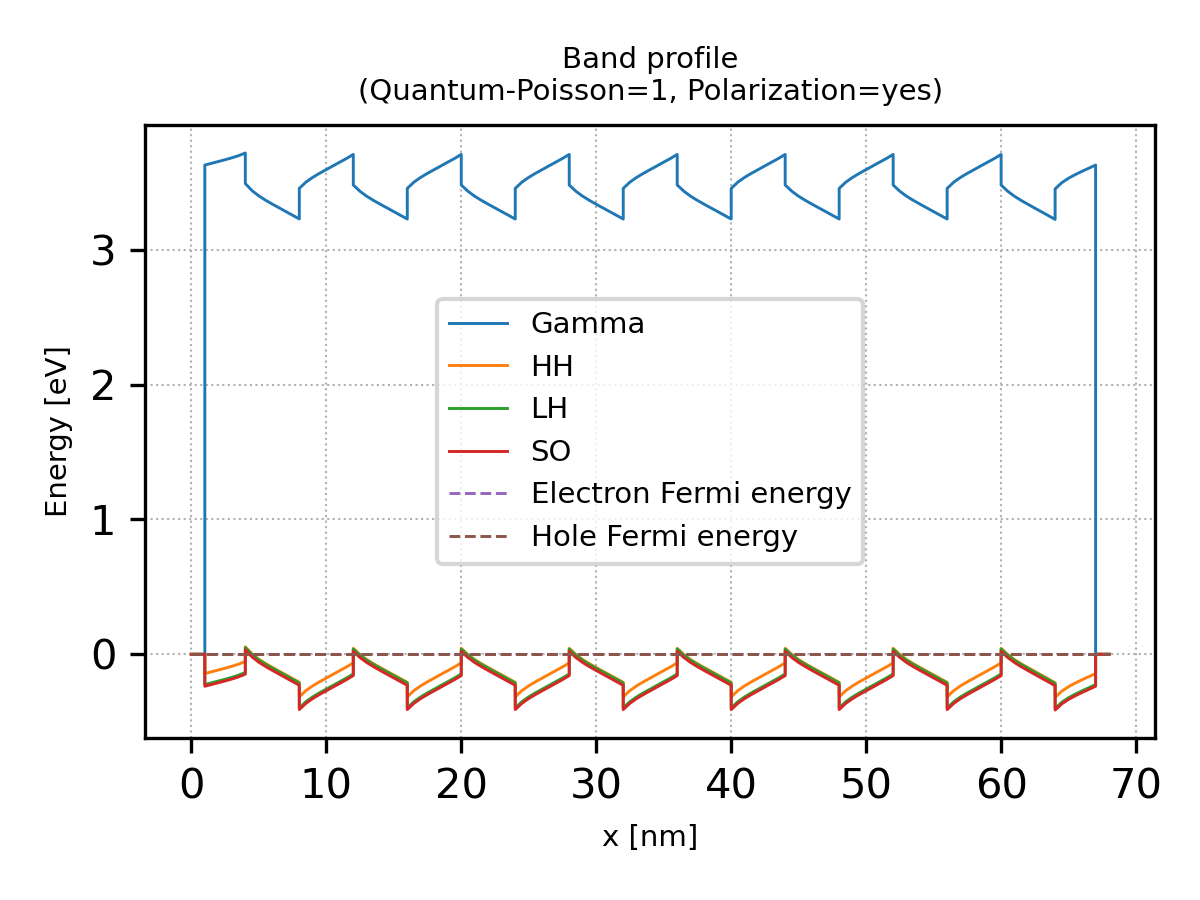
Figure 2.4.115 The band edge profile and the Fermi level
The band edge tilting is due to the piezo- and pyro-electricity, which actually enhances the acceptor ionization as can be seen later.
Scheme
Schrödinger-Poisson equation
We can specify which simulation or equations would be solved on run{ } section in your input file.
In 1D_UV_LED_KozodoyAPL1999_nnp.in it is described as
run{
    strain{ }
    poisson{ }
    quantum_poisson{ }
}
Then nextnano++ solves the strain equation and self-consistent Schrödinger-Poisson equation.
The resulting electrostatic potential \(\phi(x)\), electron density \(n(x)\), and hole density \(p(x)\) should satisfy both Poisson equation and the carrier density calculation based on Schrödinger equation. For further detailed discussion, please refer to General scheme of the optical device analysis.
Ionization of dopant
The ionized donor and acceptor densities, \(N_D^+,N_A^-\) are calculated as
where the summation is over all different donor or acceptors, \(N_D,N_A\) are the doping concentrations, \(g_D,g_A\) are the degeneracy factors (\(g_D=2\) and \(g_A=4\) for shallow impurities), and \(E_{D},E_{A}\) are the energies of the neutral donor and acceptor impurities, respectively.
These energies \(E_{D},E_{A}\) are determined by the ionization energies \(E_{D,i}^{ion},E_{A,i}^{ion}\) , the bulk conduction and valence band edges (including shifts due to strain) and the electrostatic potential as
The parameters can be specified in the input file as follows:
Doping concentrations \(N_D,N_A\) are specified at
structure{ region{ doping{} } }likestructure{ ... region{ ... doping{ #constant{ # name = "donor_impurity" # conc = 2.0e18 # cm^-3 #} constant{ name = "acceptor_impurity" conc = 5.0e19 # cm^-3 } } } }
The degeneracy factors \(g_D,g_A\) and ionization energies \(E_{D,i}^{ion},E_{A,i}^{ion}\) are specified at impurities{ } like
impurities{
    donor{
        name = "donor_impurity"    # Si
        energy = 0.030             # ionization energy measured from the conduction band edge. (fully ionized when -1000)
        degeneracy = 2             # degeneracy: 2 for n-type
    }
    acceptor{
        name = "acceptor_impurity" # Mg
        energy = 0.23              # ionization energy measured from the valence band edge. 0.23 eV is taken from Kozodoy1999. (fully ionized when -1000)
        degeneracy = 4             # degeneracy: 4 for p-type
    }
}
Results
Spatially averaged hole density
Here we show the relation between \(L=L_\text{well}=L_\text{barrier}\) and the spatially averaged hole densities.
The orange line is the result of Poisson equation ignoring the polarization fields, the blue line is the result of Poisson equation including the polarization fields, and the green line is the result of Schrödinger-Poisson equation including the polarization fields.
The corresponding hole density for bulk Al0.2Ga0.8N with the same acceptor concentration 5.0 \(\times\) 1019 [cm-3] has been calculated as around 0.43\(\times\) 1018 [cm-3], so the hole density is improved in any case.
What we can also see is that the polarization field further enhances the acceptor ionization, while the quantization effect reduces it as \(L\) becomes smaller.
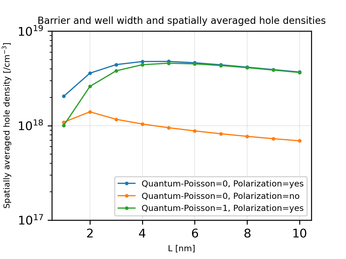
Figure 2.4.116 Barrier and well width \(L\) and spatially averaged hole densities.
Hole density/Ionized acceptor density distribution
Here we see the spatial distribution of the hole density and ionized acceptor density. We can confirm that the holes generated by the ionization of the acceptors in the barrier layers are accumulated into the well layers.
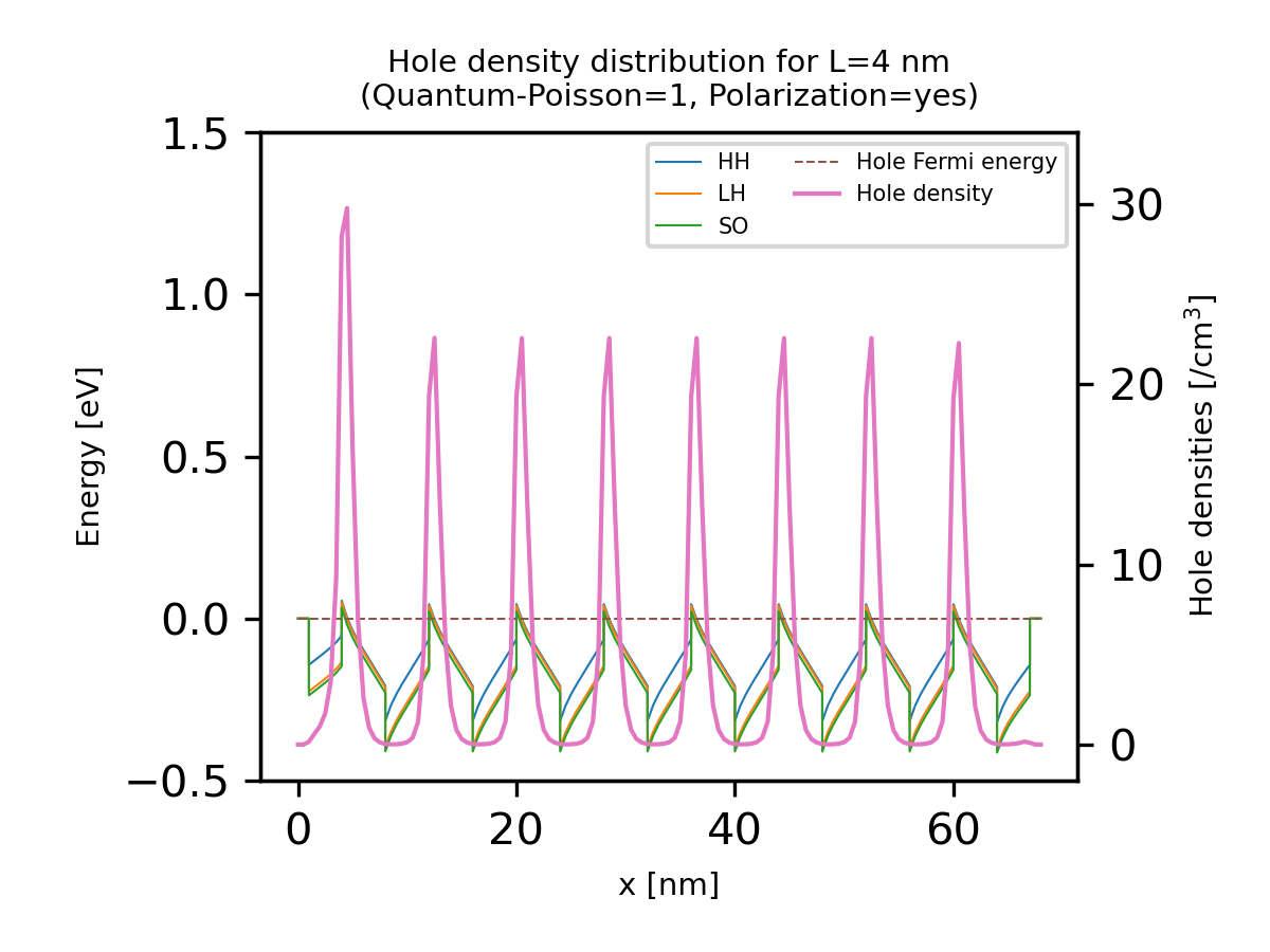
Figure 2.4.117 Hole density distribution calculated at \(L=\)4.0 nm by Schrödinger-Poisson equation including the polarization fields. The valence band edges are also displayed.
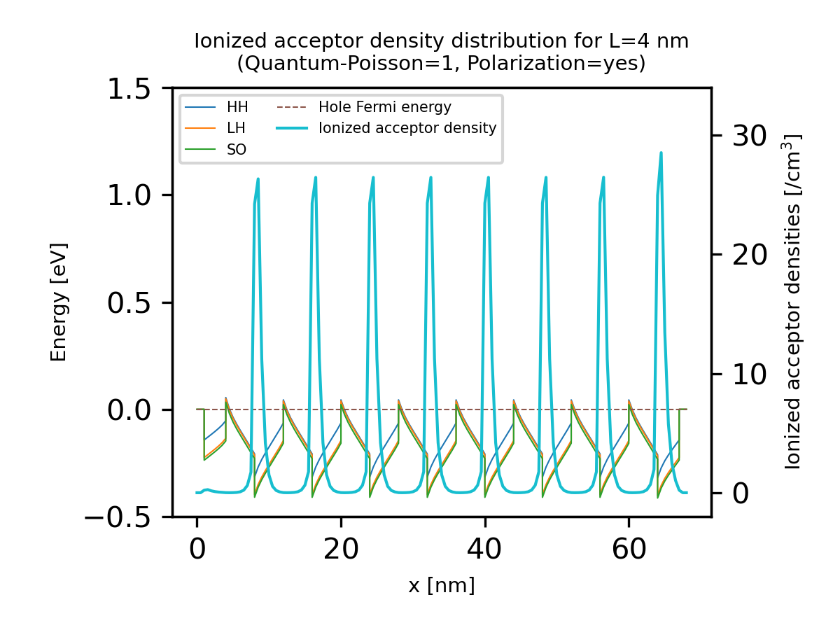
Figure 2.4.118 Ionized acceptor density distribution calculated at \(L=\)4.0 nm by Schrödinger-Poisson equation including the polarization fields. The valence band edges are also displayed.
IQE estimation
Structure
The simulation region consists of the following structure:
Material |
Thickness |
Doping |
|
n-Al0.18Ga0.82N |
100 nm |
8 \(\times\) 1018 [cm-3] (donor) |
|
In0.02Al0.09Ga0.89N - In0.02Al0.22Ga0.76N 3-layer MQW |
well: 2.5 nm, barrier: 15 nm |
0 [cm-3] |
|
Al0.24Ga0.76N/Al0.17Ga0.83N 8-layer MQW |
well: 4.0 nm, barrier: 4.0 nm |
2 \(\times\) 1019 [cm-3] (acceptor) |
|
p-Al0.17Ga0.83N as a p-contact layer | 20 nm |
2 \(\times\) 1019 [cm-3] (acceptor) |
||
The simulation result of this structure is compared with the structure where the p-region consists of bulk Al0.20Ga0.80N.
The electron blocking layer is not included here.
Bandedges
The following figures show the band edge profiles and the Fermi energies for the structures with (top) and without (bottom) SL. The width of the SL wells and barriers is set to \(L=\) 4.0 nm.
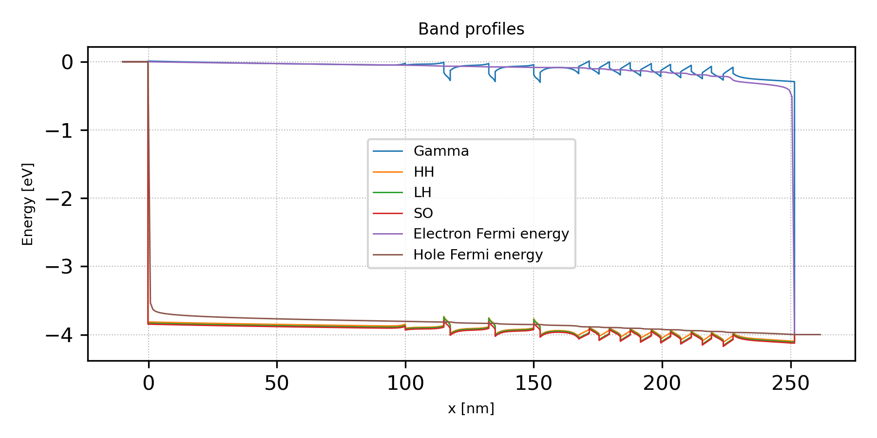
Figure 2.4.119 The band edges and Fermi levels for the structure with SL (bias=4.00 V, total current density=2.67\(\times\)105 A/cm2)
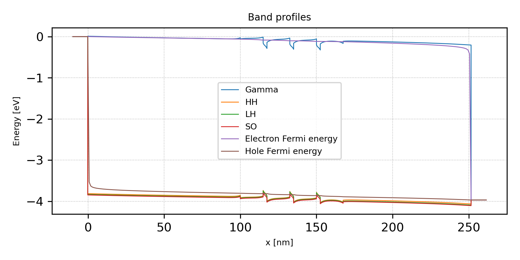
Figure 2.4.120 The band edges and Fermi levels for the structure with bulk p-region (bias=3.97 V, total current density=2.71\(\times\)105 A/cm2)
Scheme
The corresponding run{ } section is described as
run{
    strain{ }
    current_poisson{ }
}
Then nextnano++ solves the current equation and Poisson equation self-consistently after solving strain equation.
After the Current-Poisson equation has been converged, optoelectronic characteristics are calculated according to the specification in the section classical{ }.
For further details, please see General scheme of the optical device analysis.
IQE result
The calculated IQEs with respect to the applied bias (left) and current density (right) are shown here. We can see that the IQE for the structure with SL, which is slightly smaller than that of bulk at the bias around 3.4 V, becomes superior to bulk for larger biases.
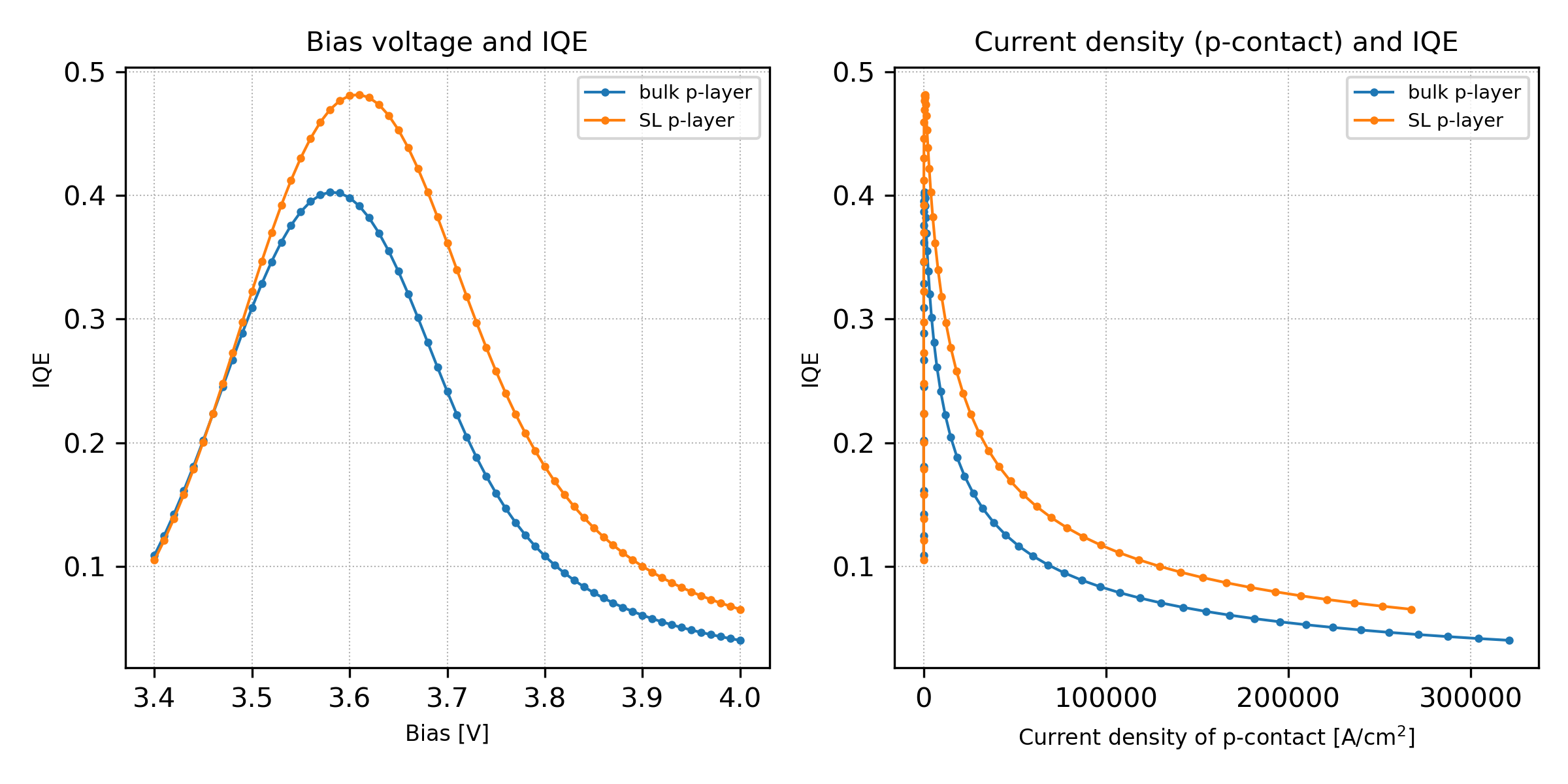
Figure 2.4.121 Left: Applied bias and IQE. Right: Current density at p-contact and IQE.
What can we do further?
By sweeping the simulation over the corresponding parameters, we can optimize the device strucutres such as \(L\), number of SLs, or the Al content of the SL region, for example. Our open source python package nextnanopy is a powerful tool for this purpose.
The graphs shown in this tutorial are also generated by a python script using nextnanopy.
Last update: nn/nn/nnnn