Dispersion in infinite superlattices: Minibands (Kronig-Penney model)
- Input files:
1Dsuperlattice_dispersion_4nm_nnpp.in
1Dsuperlattice_dispersion_6nm_nnpp.in
1Dsuperlattice_dispersion_bulk_GaAs_nnpp.in
Superlattice_1D_nnpp.in
- Scope:
This tutorial aims to reproduce two figures (Figs. 2.27, 2.28, p. 56f) of [HarrisonQWWD2005], thus the following description is based on the explanations made therein.
Superlattice 1: 4 nm \(AlGaAs\) / 4 nm \(GaAs\)
Input file: 1Dsuperlattice_dispersion_4nm_nnpp.in
Our infinite superlattice consists of a 4 nm \(GaAs\) quantum well surrounded by 2 nm \(Al_{0.4}Ga_{0.6}As\) barriers on each side. The choice of periodic boundary conditions leads to the following sequence of identical quantum wells: 4 nm \(AlGaAs\) / 4 nm \(GaAs\) / 4 nm \(AlGaAs\) / 4 nm \(GaAs\) / … . So our superlattice period has the length \(L\) = 8 nm. (Actually it has the length L = 8.25 due to the grid point resolution of 0.25 nm.)
Figure 2.4.279 shows the conduction band edge and the first eigenstate that is confined inside the well and its corresponding charge density (\(\Psi^2\)) for the superlattice vector \(k_z\) = 0. Note that periodic boundary conditions are employed for solving the Schrödinger equation. The second eigenstate is not confined inside the well and is therefore not shown here. (Note that the energies were shifted so that the conduction band edge of \(GaAs\) equals 0 eV.)
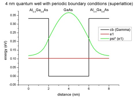
Figure 2.4.279 Calculated conduction band edge profile of single 4 nm GaAs QW with periodic boundary conditions.
In a superlattice the electrons (and holes) see a periodic potential which is similar to the periodic potential in bulk crystals. This means that the particle wave functions are no longer localized in one quantum well. They extend to infinity, and they are equally likely to be found in any of the quantum wells. The eigenstates are called Bloch states (as in bulk) and the wave functions are periodic:
For a travelling wave of the form \(exp(ik_xx)\) it holds that
\(k_x\) is the wave vector of the electron (or hole) along the growth direction of the infinite superlattice. In Figure 2.4.280 we plot the dispersion curve, i.e. the energy of the electron as a function of its superlattice wave vector \(k_x\) for the lowest eigenstate. As the energy is a periodic function of \(k_x\) with period 2\(\pi / L\), we plot only the interval [\(-\pi/L\), \(\pi/L\)].
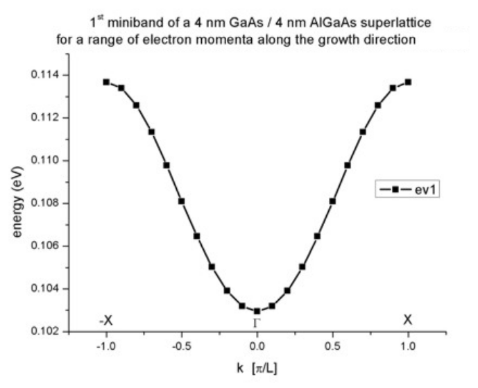
Figure 2.4.280 Calculated subband dispersion (= miniband)
The plot is in excellent agreement with Fig. 2.27 (page 56) of [HarrisonQWWD2005]. When the electron is at rest (\(k_x\) = 0), the dispersion curve shows a minimum. As the electron momentum \(k_x\) increases, its energy also increases and reaches a maximum at \(k_x\) = \(-\pi/L\) and \(k_x\) = \(+\pi/L\). Thus, the electron within the superlattice occupies a continuum of energies. This continuum that is bound by a maximum and a minimum of energy is called miniband. Due to the similarity with the energy bands of a bulk crystal, the point in the superlattice Brillouin zone for \(k_x\) = 0 is called Gamma and for \(k_x\) = \(\pi/L\) it is called X.
Superlattice 2: 6 nm \(AlGaAs\) / 6 nm \(GaAs\)
Input file: 1Dsuperlattice_dispersion_6nm_nnpp.in
Our second infinite superlattice consists of a 6 nm \(GaAs\) quantum well surrounded by 3 nm \(Al_{0.4}Ga_{0.6}As\) barriers on each side. The choice of periodic boundary conditions leads to the following sequence of identical quantum wells: 6 nm \(AlGaAs\) / 6 nm \(GaAs\) / 6 nm \(AlGaAs\) / 6 nm \(GaAs\) / … . So our superlattice period has the length \(L\) = 12 nm. (Actually it has the length \(L\) = 12.25 due to the grid point resolution of 0.25 nm.)
Figure 2.4.281 shows the conduction band edge and the two lowest eigenstates that are confined inside the well and their corresponding probailiy density (\(\Psi^2\)) for the superlattice vector \(k_x\) = 0. Note that periodic boundary conditions are employed for solving the Schrödinger equation. The third eigenstate is not confined inside the well and is therefore not shown here. In contrast to the 4 nm quantum well superlattice described above, two confined electron states exist. (Note that the energies were shifted so that the conduction band edge of \(GaAs\) equals 0 eV.)
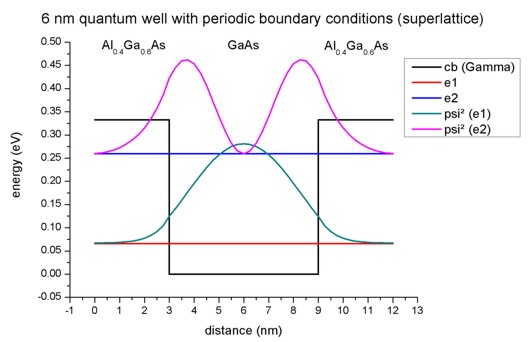
Figure 2.4.281 Calculated conduction band edge profile of single 6 nm \(GaAs\) QW with periodic boundary conditions.
The following figure (Figure 2.4.282) shows the first two minibands for this superlattice. They arise from the first and the second eigenstate. Note that due to the scale of this figure the first miniband looks almost flat. It is also interesting that for the second miniband the minimum is not at the center (i.e. at Gamma) but at the edges of the superlattice Brillouin zone at X (and -X).
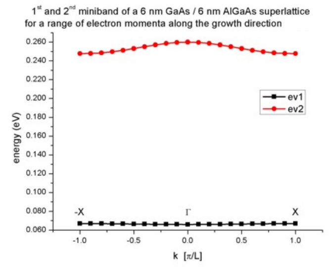
Figure 2.4.282 Calculated subband dispersion (= miniband)
Again, the plot is in excellent agreement with Fig. 2.28 (page 57) of [HarrisonQWWD2005].
Technical details
The resolution of the miniband plot has to be specified within the group quantum{ region{ dispersion{} } }:
quantum{
    region{
        ...
        dispersion{
            output_dispersions{}
            path{
                name = "superlattice_dispersion"
                point{ k = [$left_dispersion,  0.0, 0.0] }
                point{ k = [$right_dispersion, 0.0, 0.0] }
                num_points = $num_points_dispersion         # number of superlattice vectors along x direction
            }
        }
    }
}
For each superlattice vector \(k_x\), the Schrödinger equation has to be solved. The 11th superlattice vector corresponds to \(k_x\) = 0 which is obviously identical to the case when no superlattice is specified at all. The miniband dispersion is written to this file: dispersion_quantum_region_Gamma_superlattice_dispersion.dat.
Dispersion in bulk \(GaAs\)
Input file: 1Dsuperlattice_dispersion_bulk_GaAs_nnpp.in
The input file is basically equivalent to 1Dsuperlattice_dispersion_6nm_nnpp.in, except that we replace the \(AlGaAs\) barrier with \(GaAs\) so that we have only pure bulk \(GaAs\) with a length of 12 nm. So our superlattice period has the length \(L\) = 12 nm. (Actually it has the length \(L\) = 12.25 due to the grid point resolution of 0.25 nm.) At the boundaries we apply periodic boundary conditions and the same superlattice options (number of \(k\) values and direction in \(k\) space) as above.
Figure 2.4.283 shows the conduction band edge and the three lowest eigenstates and their corresponding probability density (\(\Psi^2\)) for the superlattice vector \(k_x\) = 0. Note that periodic boundary conditions are employed for solving the Schrödinger equation.
The ground state wave function is constant with its energy equal to the conduction band edge energy.
The energies of the second and third eigenstate are degenerate.
(Note that the energies were shifted so that the conduction band edge of \(GaAs\) equals 0 eV.)
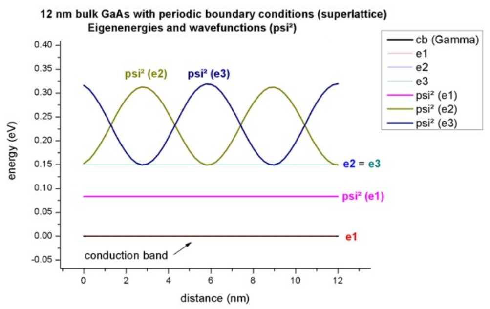
Figure 2.4.283 Calculated conduction band edge profile of bulk \(GaAs\) and \(\Psi^2\) of lowest electron eigenstates (periodic boundary conditions were used).
The following figure (Figure 2.4.284) shows the first three minibands for this superlattice. They arise from the first, second and third eigenstate. The second and third eigenstate are degenerate at \(k_x\) = 0 as can be seen also in the figure above. Also at \(k_x\) = -1 and \(k_x\) = 1, the first and second eigenstate are degenerate. This is as expected because the dispersion should look like the parabolic dispersion \(E(k)\) of bulk \(GaAs\).
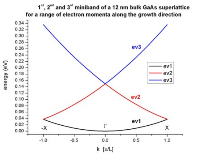
Figure 2.4.284 Calculated subband dispersion (= miniband)
Template
Input file: Superlattice_1D_nnpp.in
We want to study the energy levels of a superlattice in order to understand how they form bands in a periodic structure. One can easily see this by calculating the energy levels for various barrier heights, i.e. we automatically generate input files for the variable “Barrier_Height”. Once done, we visualize the subband dispersions contained in the file dispersion_quantum_region_Gamma_superlattice_dispersion.dat.
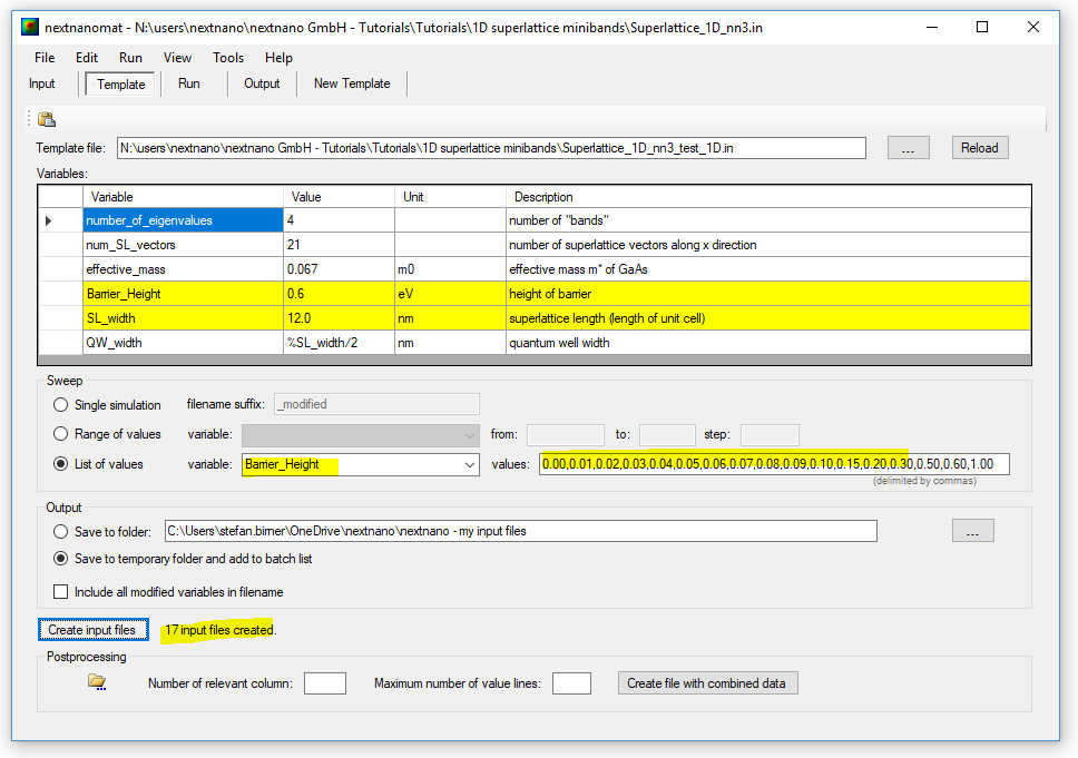
Figure 2.4.285 compares the dispersion of a superlattice for two different QW barrier heights.
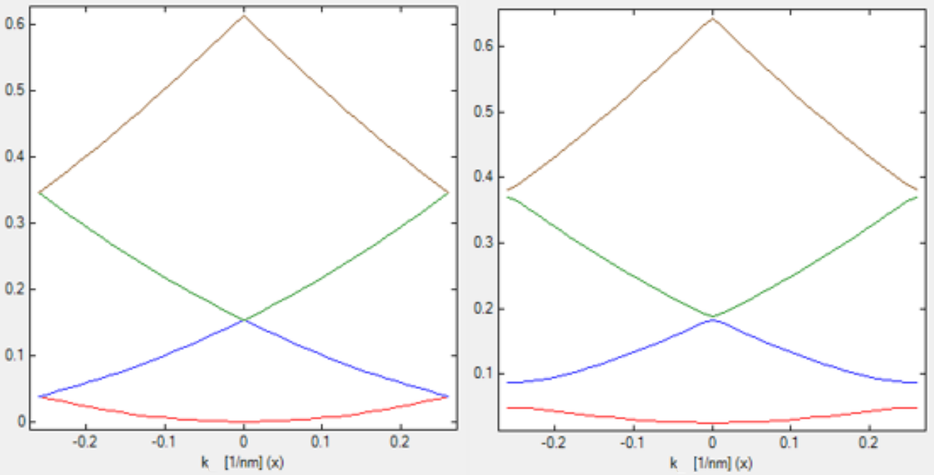
Figure 2.4.285 The left figure contains a quantum well superlattice with a barrier height of 0 eV, i.e. a bulk semiconductor, while the figure on the right shows the dispersion for a barrier height of 0.06 eV.
Last update: nn/nn/nnnn