UV LED: Quantitative evaluation of the effectiveness of EBL
Header
- Files for the tutorial located in nextnano++\examples:
1D_DUV_LED_HirayamaJAP2005_EBL_nnp.in
We investigate how the electron blocking layer (EBL) improves the characteristics of UV LEDs using nextnano++. Current-Poisson equation and semi-classical calculation of optical properties (classical{ }) in nextnano++ enables us to quantitatively analyze the effect of this strucutre.
We refer to the structure used to obtain Fig. 28 in the [HirayamaJAP2005]:
Structure
The simulation region consists of the following structure:
n-Al0.18Ga0.82N layer
3-layer MQW based on InAlGaN
AlxGa1-xN EBL (Al content = 0.18, 0.24, 0.28)
p-Al0.18Ga0.82N layer
Each layer has the following thickness and doping concentration:
Material |
Thickness |
Doping |
n-Al0.18Ga0.82N |
100 nm |
8 \(\times\) 1018 [cm-3] (donor) |
In0.02Al0.09Ga0.89N - In0.02Al0.22Ga0.76N 3-layer MQW |
well: 2.5 nm, barrier: 15 nm |
0 [cm-3] |
AlxGa1-xN EBL with x=0.28, 0.24, 0.18 |
10 nm |
0 [cm-3] for x=0.28, 0.24, 2 \(\times\) 1019 [cm-3] for x=0.18 (acceptor) |
p-Al0.18Ga0.82N |
100 nm |
2 \(\times\) 1019 [cm-3] (acceptor) |
Al content x=0.18 in the EBL is used for the structure without EBL, while x=0.24 and 0.28 are for the structure with EBL in different barrier height.
Donor and acceptor ionization energies are defined as 0.030 eV and 0.158 eV where Si and Mg are in mind, respectively.
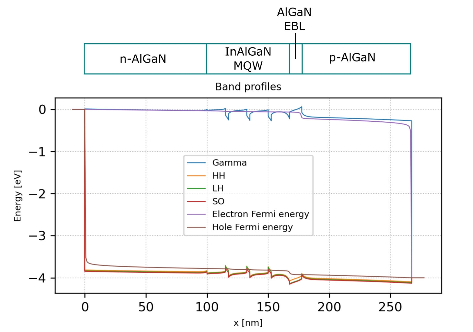
Figure 2.4.4.18 The band edges and Fermi levels for the structure with higher EBL (x=0.28, bias=4.00V, total current density=1.67\(\times\)105 A/cm2)
Scheme
We can specify which simulation or equations would be solved on run{ } section in your input file.
In 1D_DUV_LED_HirayamaJAP2005_EBL_nnp.in it is described as
run{
    strain{ }
    current_poisson{ }
}
Then nextnano++ solves the current equation and Poisson equation self-consistently after solving strain equation.
After the Current-Poisson equation is converged, optoelectronic characteristics are calculated according to the specification in the section classical{ }.
For further details, please see General scheme of the optical device analysis.
Results
Current-voltage characteristics
Here we show the current-voltage characteristics for the total current density \(I_{\text{total}}\) measured at p-contact and photocurrent density \(I_{\text{photo}}\), which is defined as (2.2.5.28). \(I_{\text{photo}}\) represents the amount of electrical current consumed by the radiative recombination in the total current \(I_{\text{total}}\). Please note that the scales of the y-axis in these graphs are different in 10 times.
We can observe that the smaller \(I_{\text{total}}\) is , the higher the EBL barrier is. On the other hand, at the applied bias of 4.0V, the bigger \(I_{\text{photo}}\) is, the higher the EBL barrier is. We can say that the larger proportion of the total current consists of the photocurrent in the higher EBL structure, which results in the larger IQE.
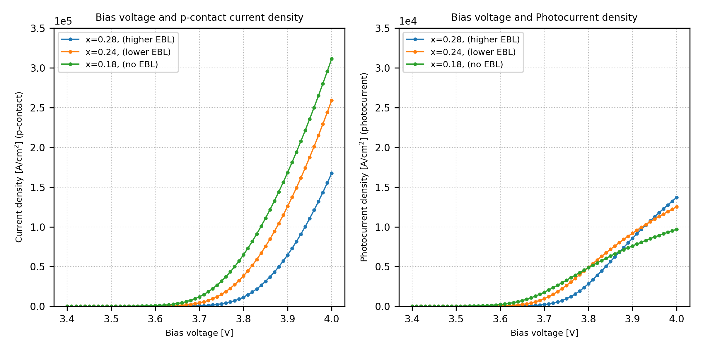
Figure 2.4.4.19 (Left:) The relationship between the p-contact current density and bias voltage. (Right:) The relationship between the photocurrent \(I_{photo}\) and bias voltage.
Bandedges
The following figures show the band edge profiles and the quasi-Fermi levels for the higher EBL (top) and no EBL (bottom) structure where the total current densities are almost the same around 1.70 \(\times\) 105 A/cm2. The applied bias is 4.00 V for the left graph and is 3.90 V for the right graph.
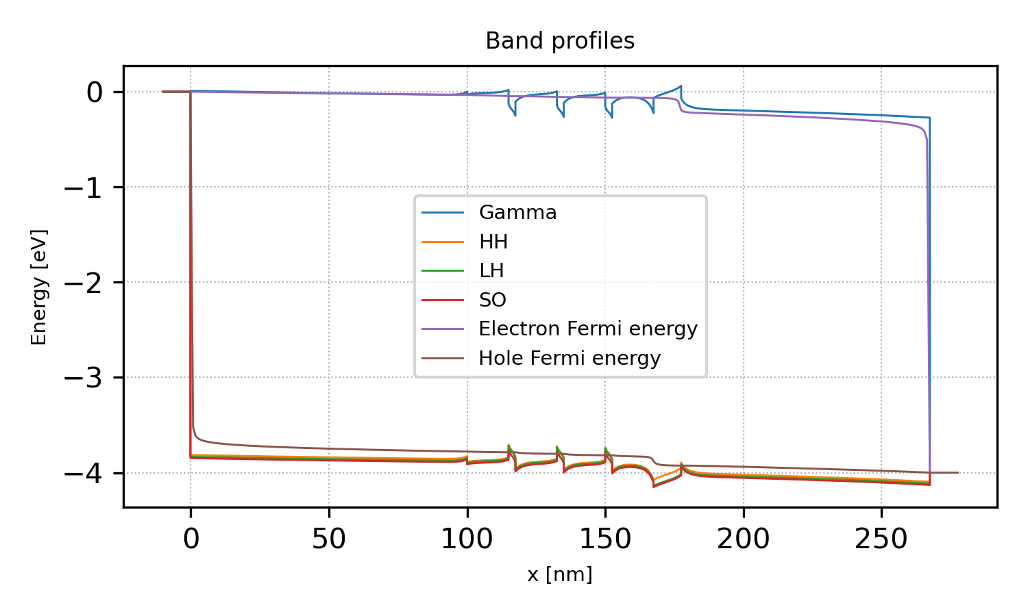
Figure 2.4.4.20 The band edges and Fermi levels for the structure with EBL (x=0.28, bias=4.00V, total current density=1.67\(\times\)105 A/cm2)
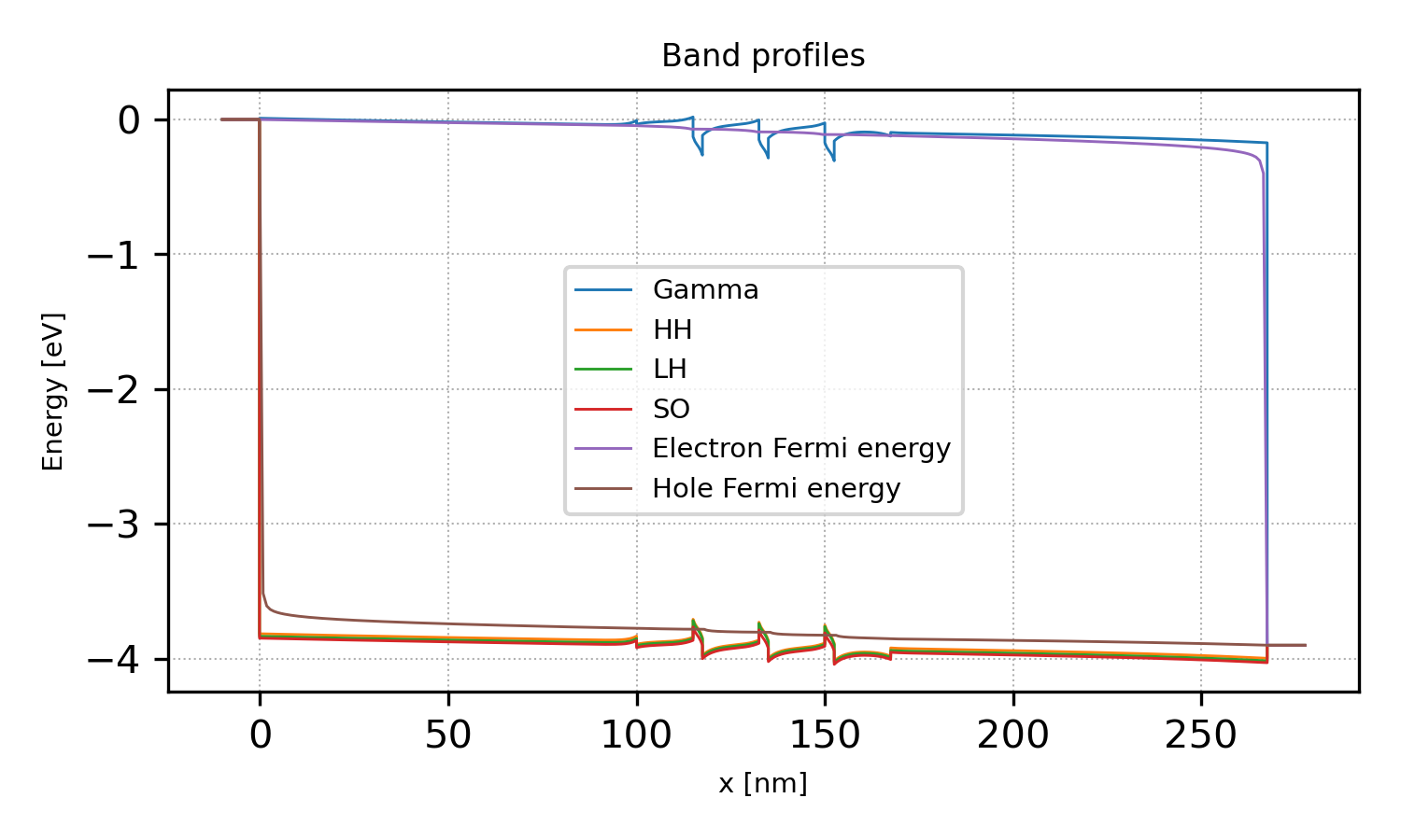
Figure 2.4.4.21 The band edges and Fermi levels for the structure without EBL (x=0.18, bias=3.90V, total current density=1.68\(\times\)105 A/cm2)
Current Density
The following figure show the current density profiles for the higher EBL (top, x=0.28), lower EBL (middle, x=0.24), and no EBL (bottom, x=0.18) structure where the total current densities are almost the same around 1.70 \(\times\) 105 A/cm2.
We can see that the amount of electron current and hole current becomes closer as the EBL height is increased, while the electron current is dominant without EBL. It can be also confirmed that the current overflow is suppressed by the EBL.
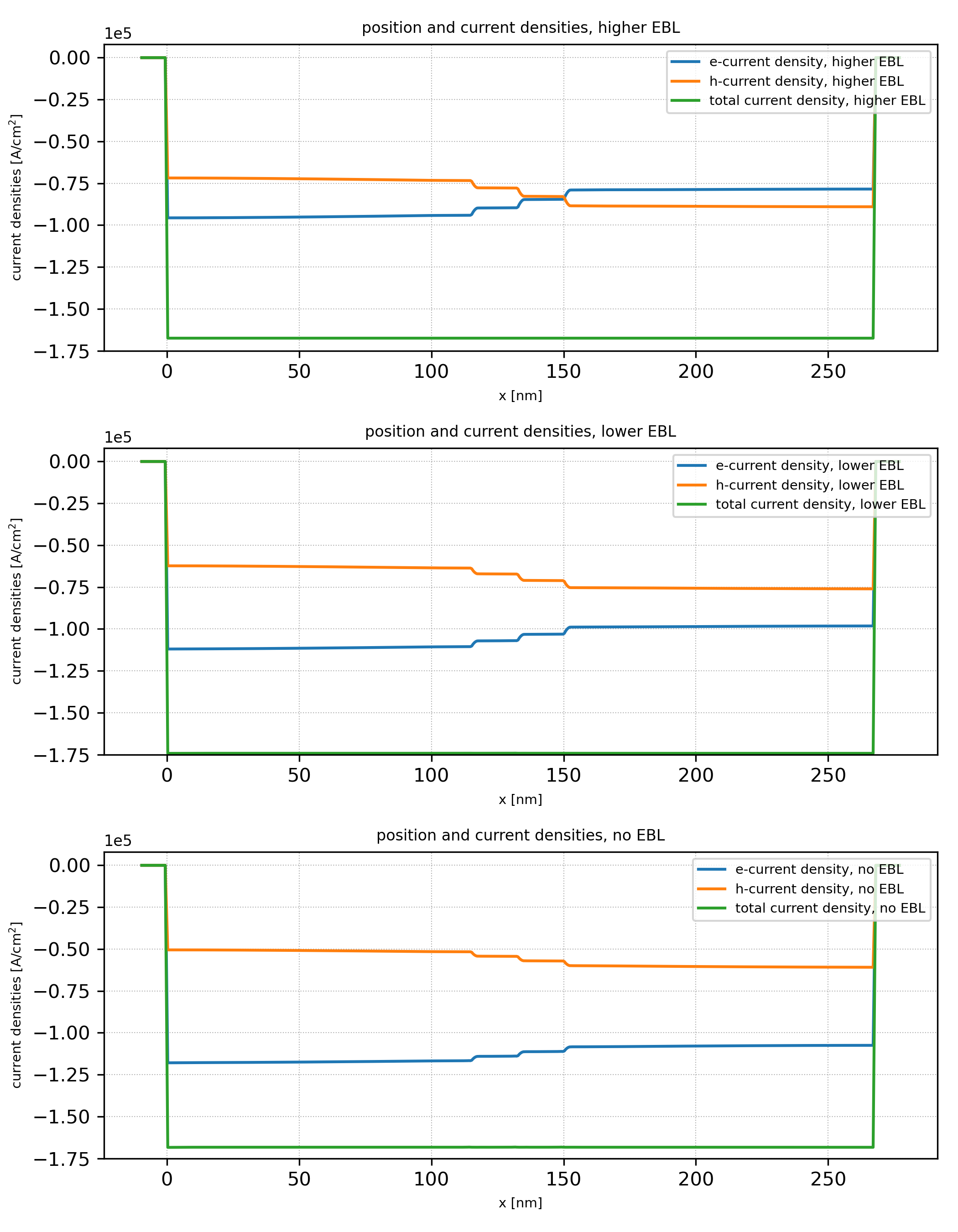
Figure 2.4.4.22 The current density profile for the the structures with higher EBL (top, 4.00 V, 1.67\(\times\) 105 A/cm2), lower EBL (middle, 3.94 V, 1.74\(\times\) 105 A/cm2), and no EBL (bottom, 3.90 V, 1.68\(\times\) 105 A/cm2).
Charge carrier densities
The figures showed below are the electron and hole densities around the MQW region for the structure with higher EBL and without EBL (left, x=0.28 and right, x=0.18) for almost the same current density around 1.70 \(\times\) 105 A/cm2. The introduction of EBL at 167 nm-177 nm reduces the electron densitiy in the p-AlGaN region.
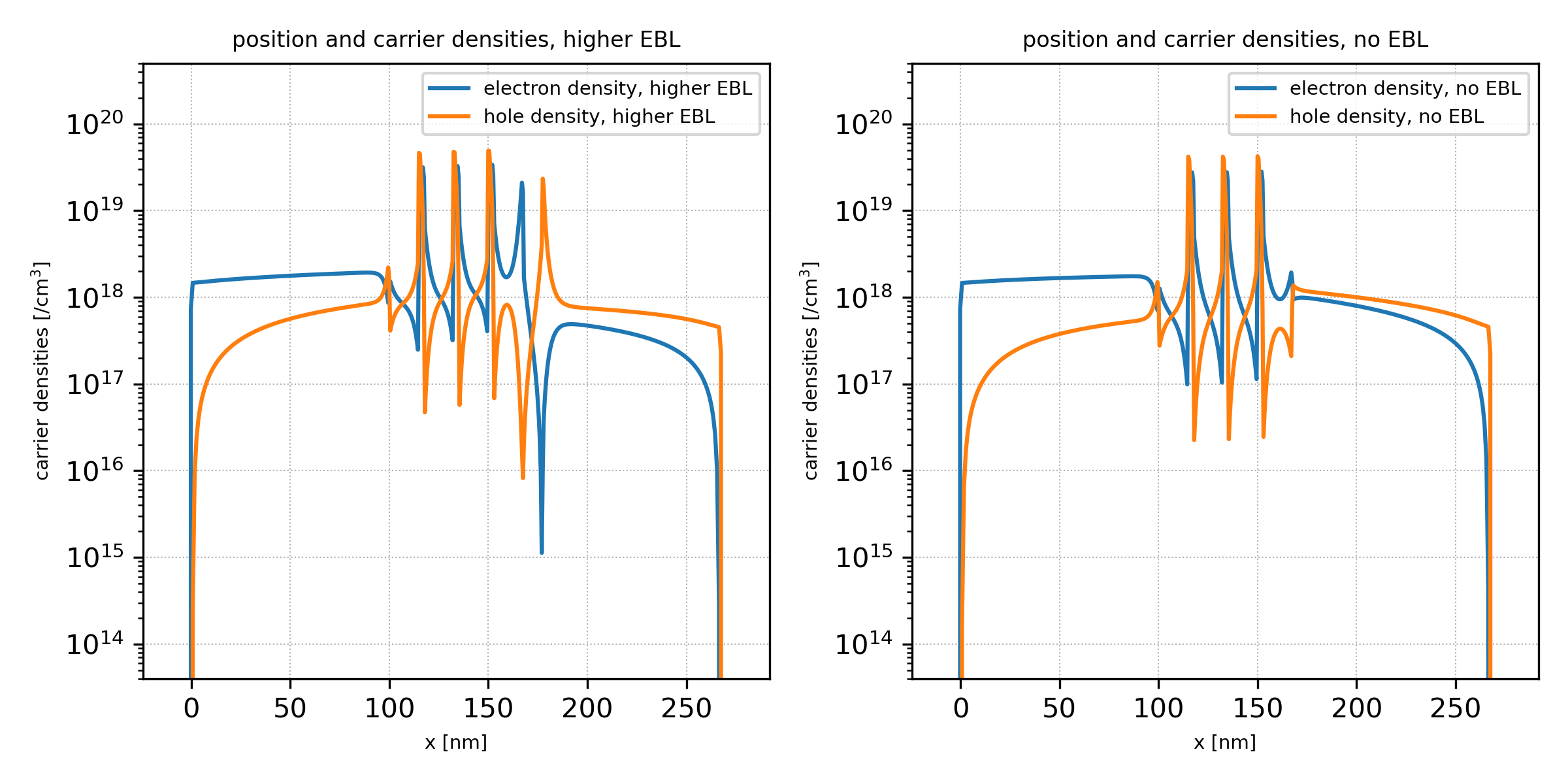
Figure 2.4.4.23 The electron and hole densities calculated in the structures with higher EBL (left, 4.00 V, 1.67\(\times\) 105 A/cm2) and no EBL (right, 3.90 V, 1.68\(\times\) 105 A/cm2).
Power of light emission
Here we show the relationship between optical power defined in (2.2.5.33) and current density of p-contact for each structure.
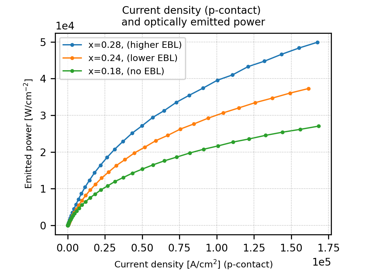
Figure 2.4.4.24 Current vs. power of light emission
Internal quantum efficiency
In nextnano++, the internal quantum efficiency is calculated as
where \(I_\text{photo}\) is the photo-urrent consumed by the radiative recombination and \(I_\text{total}\) is the current injected in total.
This quantity shows the improvement by the introduction of higher EBL as follows:
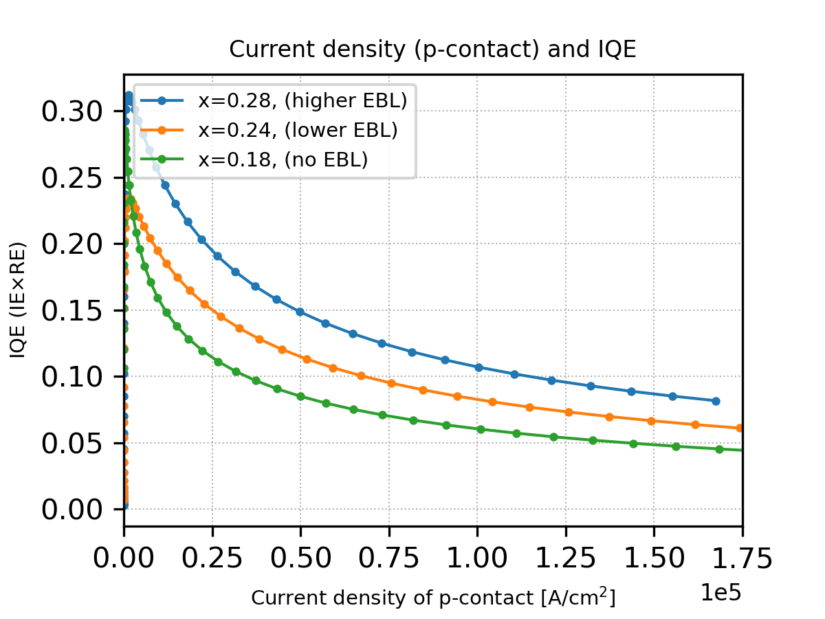
Figure 2.4.4.25 Current and internal quantum efficiency (IQE).
The nextnano++ tool also outputs the volume quantum efficiency \(\eta_\text{VQE}\), also known as radiative efficiency, which represents the proportion of the radiative recombination rate to the total recombination rate. This quantity is calculated as
and also shows the improvement by the introduction of EBL:
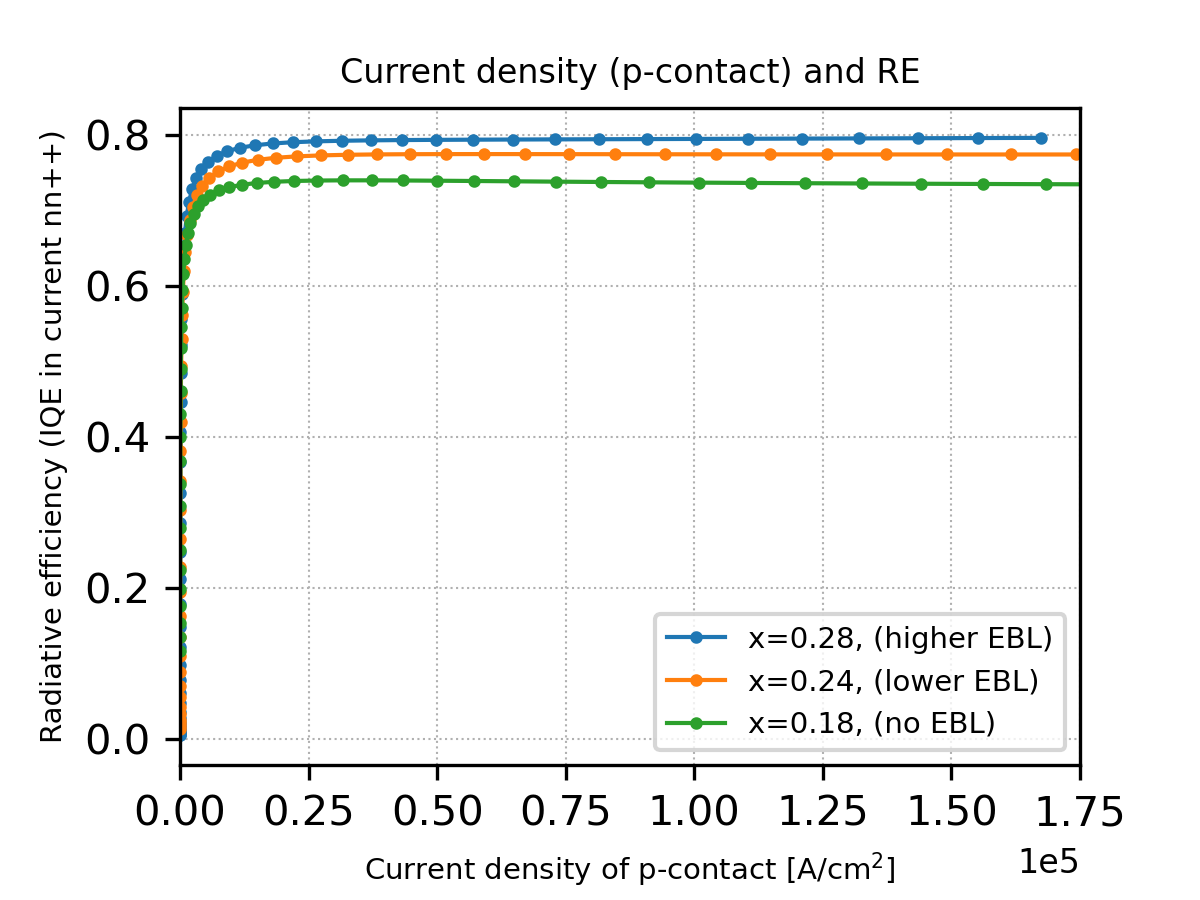
Figure 2.4.4.26 Current and volume quantum effciency (radiative efficiency).
The IQE can be decomposed like (2.4.4.8) into this volume QE and the injection efficiency \(\eta_\text{IE}\), which represents the proportion of the current consumed by the total recombination (radiative + nonradiative) to the total injected current.
Thus using the results of \(\eta_\text{IQE}\) and \(\eta_\text{VQE}\) above, we can also get this \(\eta_\text{IE}\) :
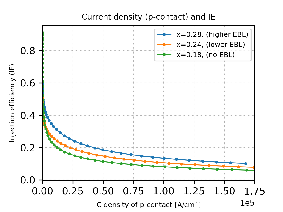
Figure 2.4.4.27 Current and injection efficiency (IE).
From the above results, we can see that the improvement of IQE due to the introduction of EBL comes from the imrovement of mainly IE rather than volume QE.
What can we do further?
The effect of EBL on the optoelectronic characteristics has been estimated quantitatively using the semiclassical calculation in nextnano++.
We can also optimize the Al content of EBL or the thickness by sweeping the corresponding parameters, for example. Our open source python package nextnanopy is a strong tool for this purpose.
The graphs shown in this tutorial are also generated by a python script using nextnanopy.
Last update: 16/07/2024