Two-dimensional electron gas in an AlGaN/GaN FET
- Input files:
Jogai_AlGaNGaN_FET_JAP2003_noGaNcap_Fig4Fig1Fig7_1D_nnp.in
Jogai_AlGaNGaN_FET_JAP2003_noGaNcap_Fig2Fig3_1D_nnp.in
Jogai_AlGaNGaN_FET_JAP2003_GaNcap_Fig4_1D_nnp
Jogai_AlGaNGaN_FET_JAP2003_GaNcap_Fig6Fig5_1D_nnp.in
Note
The input files are also available as 2D input file.
- Scope:
This tutorial tries to reproduce the results of [Jogai2003].
Introduction
For this one-dimensional simulation of an \(AlGaN\)/ \(GaN\) heterojunction field effect transistor (HFET) we are solving self-consistently the Schrödinger-Poisson equation taking into account strain, and piezo- and pyroelectric charge densities.
At the left boundary we use a Schottky contact boundary condition with a Schottky barrier height of \(\phi_B\) = 1.4 eV. Note that in Fig. 1 of [Jogai2003], the Schottky barrier height corresponds to
which fixes the conduction band edge energy \(E_c\) above the Fermi energy \(E_F\), where \(\mathrm{e}\) is the elementary charge. Alternative boundary conditions such as a fixed surface charge density or surface states based on incomplete ionization of donor or acceptor states are described in the Schottky barrier tutorial.
Our simulated structure is undoped. Note that the 2DEG is present even in the absence of doping due to piezo- and pyroelectric interface charge densities. The temperature is set to 300 K in all simulations. We only consider cation-faced structures, i.e. we have rotated the crystal so that our [000-1] direction points along the positive x direction.
Figure 2.4.15.3 shows the results of the input file 1DJogai_AlGaNGaN_FET_JAP2003_noGaNcap_Fig4Fig1Fig7_nnp.in.
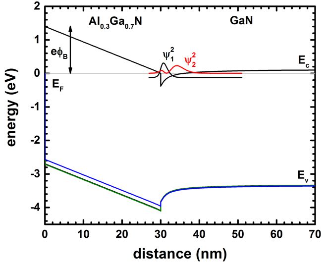
Figure 2.4.15.3 Calculated conduction and three valence band edges with the probability densities of the two lowest subbands of a 30 nm \(Al_{0.3}Ga_{0.7}N\) / 40 nm \(GaN\) heterostructure.
Variation of the \(Al_xGa_{1-x}N\) layer thickness and alloy content \(x\) (Fig. 2 and Fig. 3 of [Jogai2003])
Now we try to reproduce Fig. 2 and Fig. 3 of [Jogai2003], with the input file Jogai_AlGaNGaN_FET_JAP2003_noGaNcap_Fig2Fig3_1D_nnp.in. We are calculating the variation of the 2DEG density with the
\(Al_xGa_{1-x}N\) layer thickness and
mole fraction (alloy content \(x\)).
Within the nextnano++ input file, we can perform a sweep over the alloy concentration very conveniently:
$AlloySweepActive = yes # sweep alloy concentration from 0.4 to 0.0 (HighlightInUserInterface)
The thickness of the \(Al_xGa_{1-x}N\) barrier is defined as a variable.
$ThicknessAlGaN = 30.0 # thickness of AlGaN spacer (ListOfValues:6,10,14,18,22,26,30,34,38)(DisplayUnit:nm)(HighlightInUserInterface)
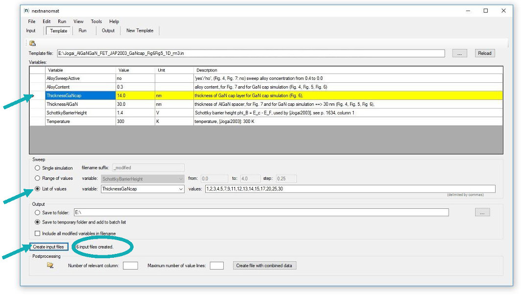
We use nextnanomat’s Template feature in order to sweep over the \(Al_xGa_{1-x}N\) barrier thickness. This is shown in the following screenshot. The input files are created automatically and are added to the “Run” tab.
The 2DEG sheet carrier concentration can be found in this file: bias_00000\total_charges.txt. This file contains the integrated electron density for the whole simulation region.
The following figure shows the total integrated electron density as a function of alloy concentration for various \(AlGaN\) thicknesses. Note that these results were obtained by using one input file template only: 1DJogai_AlGaNGaN_FET_JAP2003_nn3_Fig2Fig3.in.
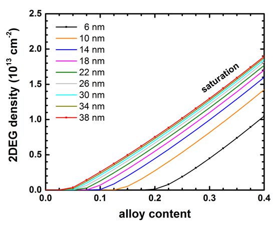
Figure 2.4.15.4 Calculated 2DEG density for different layer widths of \(Al_xGa_{1-x}N\) as a function of alloy content \(x\).
For a given barrier thickness, the 2DEG sheet carrier concentration varies almost linearly with alloy concentration \(x\). The 2DEG density approaches saturation as the barrier thickness is increased. This fact can be better seen Figure 2.4.15.5 where we show exactly the same data.
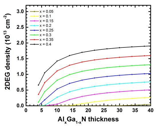
Figure 2.4.15.5 Calculated 2DEG density for different alloy contents \(x\) of \(Al_xGa_{1-x}N\) as a function of layer widths.
Our results seem to be in reasonable agreement to the simulations of [Jogai2003] (Fig. 2 and Fig. 3).
Variation of the Schottky barrier height (Fig. 7 of [Jogai2003])
Using te input file Jogai_AlGaNGaN_FET_JAP2003_noGaNcap_Fig4Fig1Fig7_1D_nnp.in, we vary the Schottky barrier height \(phi_B\) and calculate for each value the 2DEG density:
$SchottkyBarrierHeight = 1.4 # Schottky barrier height phi_B = E_c - E_F, used by [Jogai2003], see p. 1634, column 1 (ListOfValues:1.40,1.42,1.65)(RangeOfValues:From=0.0,To=4.0,Step=0.25)(DisplayUnit:V)
This situation is equivalent to fixing the surface potential to
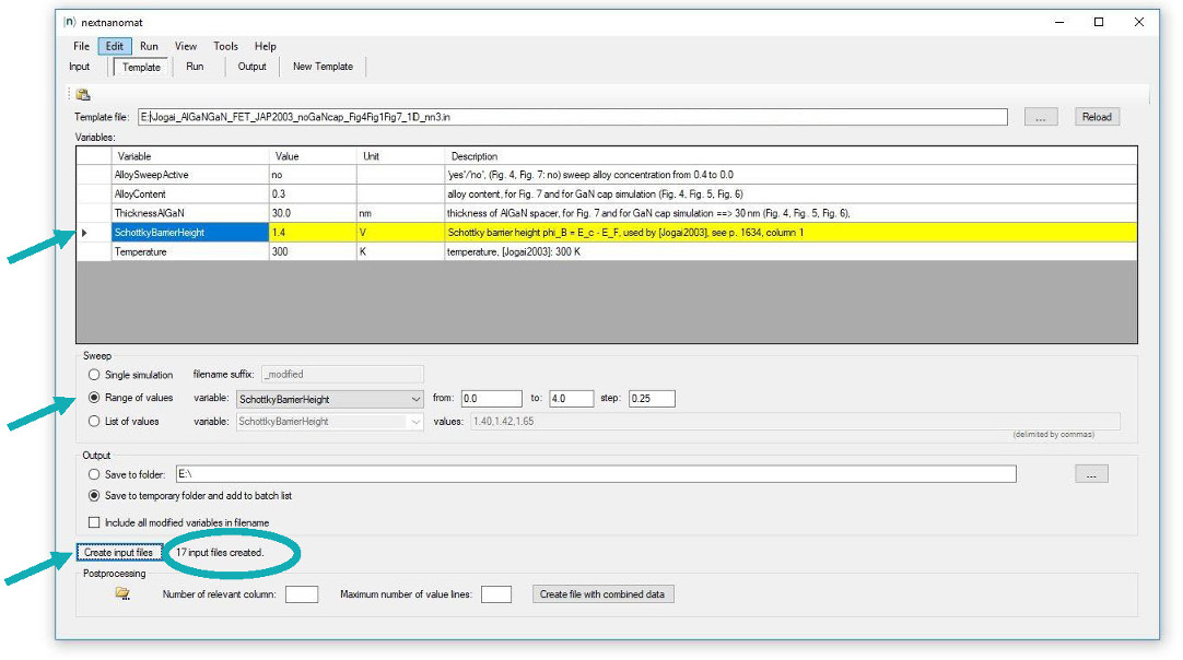
Figure 2.4.15.6 shows the calculated 2DEG density as a function of Schottky barrier height, i.e. surface potential. We used a 30 nm \(Al_{0.3}Ga_{0.7}N\) barrier. Again, the 2DEG sheet carrier concentration can be found in this file: bias_00000\total_charges.txt. The results are in reasonable agreement to Fig. 7 of [Jogai2003].
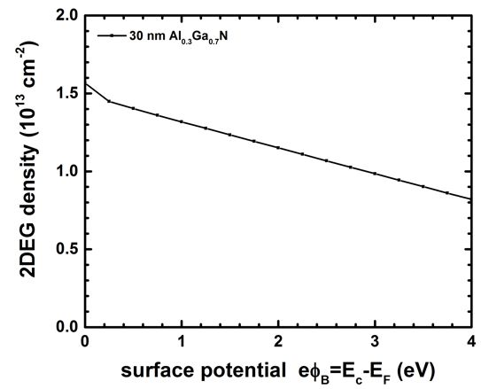
Figure 2.4.15.6 Calculated 2DEG density as a function of surface potential \(\mathrm{e} \phi_B\).
AlGaN/GaN FET including a GaN cap layer
Now we compare HFET structures with and without a GaN cap layer by using the input files Jogai_AlGaNGaN_FET_JAP2003_GaNcap_Fig4_1D_nnp.in and Jogai_AlGaNGaN_FET_JAP2003_noGaNcap_Fig4Fig1Fig7_1D_nnp.in. GaN-capped HFETs have a lower 2DEG density compared to uncapped structures. For the case of a 30 nm \(Al_{0.3}Ga_{0.7}N\) barrier, introducing a GaN cap layer reduces the density of the 2DEG:
5 nm cap: The calculated 2DEG density is n = 1.03 \(\cdot\) 1013 cm-2 (n = 1.20 \(\cdot\) 1013 cm-2 [Jogai2003]).
without cap: The calculated 2DEG density is n = 1.25 \(\cdot\) 1013 cm-2 (n = 1.47 \(\cdot\) 1013 cm-2 [Jogai2003]).
Figure 2.4.15.7 compares the band edges of capped and uncapped HEMT structure.
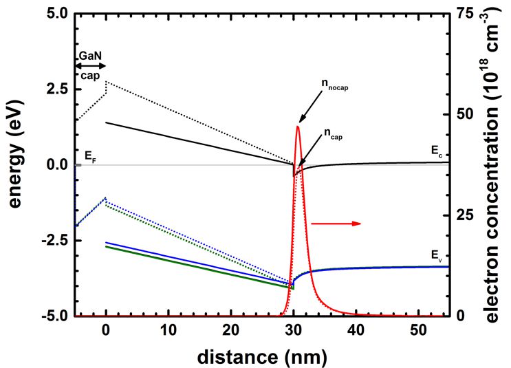
Figure 2.4.15.7 Calculated conduction and valence band edges of a \(Al_{0.3}Ga_{0.7}N\)/ \(GaN\) FET with (solid lines) and without (dotted lines) a 5 nm \(GaN\) cap layer.
Figure 2.4.15.8 shows the band edges and the electron and hole densities for a 14 nm \(GaN\) cap layer. The \(Al_{0.3}Ga_{0.7}N\) barrier thickness is 30 nm. For \(GaN\) cap layers thicker than 14 nm, a 2DHG forms. The density of the 2DHG screens the surface potential so that the density of the 2DEG is maintained at a constant level even if the \(GaN\) cap layer thickness increases further.
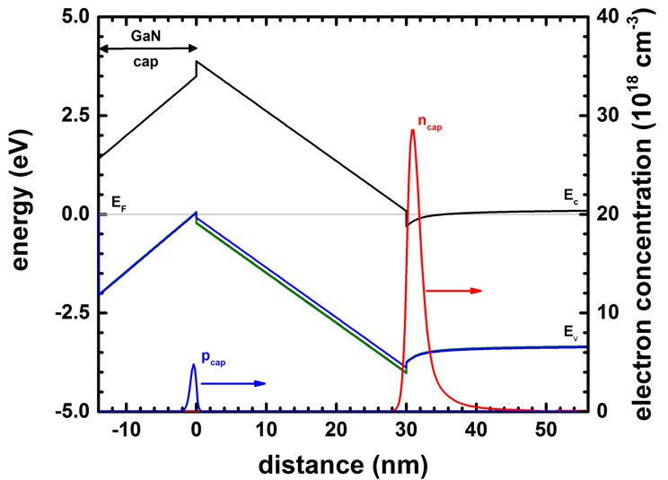
Figure 2.4.15.8 Calculated conduction and valence band edges of a \(Al_{0.3}Ga_{0.7}N\)/ \(GaN\) FET with 14 nm \(GaN\) cap.
The calculated 2DHG density is p = 0.513 \(\cdot\) 1012 cm-2 (p = 1.77 \(\cdot\) 1012 cm-2 [Jogai2003]).
The calculated 2DEG density is n = 0.839 \(\cdot\) 1013 cm-2 (n = 1.009 \(\cdot\) 1013 cm-2 [Jogai2003]).
Variation of the \(GaN\) cap layer thickness (Fig. 5 of [Jogai2003])
Input file: Jogai_AlGaNGaN_FET_JAP2003_GaNcap_Fig6Fig5_1D_nnp.in
Now we are going to vary the \(GaN\) cap layer thickness.
$ThicknessGaNcap = 5.0 # thickness of GaN cap layer for GaN cap simulation (Fig. 4, Fig. 5), (ListOfValues:1,2,3,4,5,7,9,11,12,13,14,15,17,20,25,30)(DisplayUnit:nm)(HighlightInUserInterface)
Figure 2.4.15.9 shows the 2DEG density vs. \(GaN\) cap layer thickness for a 30 nm \(Al_{0.3}Ga_{0.7}N\) barrier. Beyond a \(GaN\) cap layer thickness of ~13 nm (12 nm [Jogai2003]) the 2DEG density saturates.
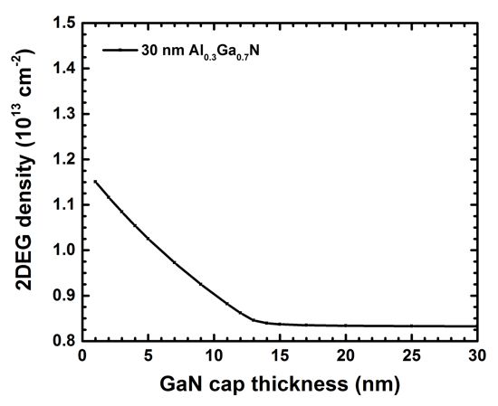
Figure 2.4.15.9 Calculated 2DEG density as a function of \(GaN\) cap thickness.
Additional comments
In contrast to the article of [Jogai2003], we did not include exchange-correlation effects and we used a single-band model for the 2DHG rather than a 6-band k.p model.
Last update: nn/nn/nnnn