Energy levels in a pyramidal shaped InAs/GaAs quantum dot including strain and piezoelectric fields
- Input files:
3DInAsGaAsQDPyramid_PryorPRB1998_10nm_nnp.in
- Scope:
In this tutorial we calculate the energy levels in a pyramidal shaped quantum dot. This tutorial is based on [Pryor1998]. We use identical material parameters with respect to this paper in order to make it possible to reproduce Pryor’s results. We note that meanwhile more realistic material parameters are available and that for the simulation of realistic quantum dots the inclusion of the wetting layer and an appropriate nonlinear \(InGaAs\) alloy profile is recommended.
- Output files:
bias_00000\bandedges_1d_x.dat
bias_00000\bandedges_1d_z.dat
bias_00000\Quantum\probability_shift_dot_Gamma_0001.avs.fld
bias_00000\Qunatum\energy_spectrum_dot_Gamma_00000.dat
bias_00000\Qunatum\energy_spectrum_dot_HH_00000.dat
Introduction
We make the following simplifications in order to be consistent with [Pryor1998]:
The wetting layer is omitted for simplicity.
The QD material is purely \(InAs\).
The barrier material is purely \(GaAs\).
The dielectric constant in the barrier material (\(GaAs\)) is the one for \(InAs\).
Periodic boundary conditions are assumed in all three directions for the strain equation.
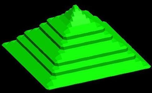
The QD shape is a pyramid with a square base (base length = 10 nm) and a height of 5 nm.
The four side walls of the pyramid are oriented in the (011), (0-11), (101) and (-101) planes, respectively.
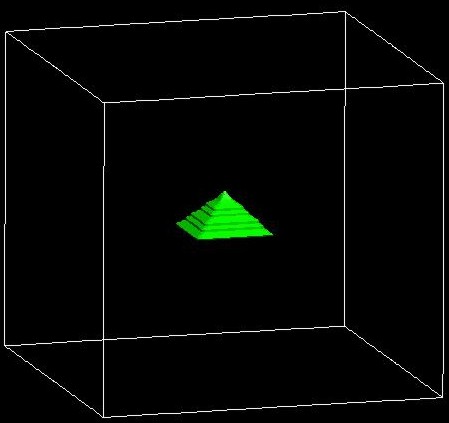
The whole simulation area has the dimensions 44 nm x 44 nm x 40 nm.
Conduction and valence band profiles
The following figures show the conduction and valence band edges (heavy hole, light hole and split-off hole) for a 10 nm pyramidal shaped QD along two different line scans. Figure 2.4.8.24 shows the band profile along the z axis through the center of the QD (x = y = 0 nm), and Figure 2.4.8.25 shows the band profile along the x axis through the base of the QD (y = z = 0 nm).
The energies of the bands have been obtained by diagonalizing the 8-band k.p Hamiltonian at \(k\) = 0 (including the Bir-Pikus strain Hamiltonian) for each grid point, taking into account the local strain tensor and deformation potentials. Note that piezoelectric effects are not included yet in this band profile.
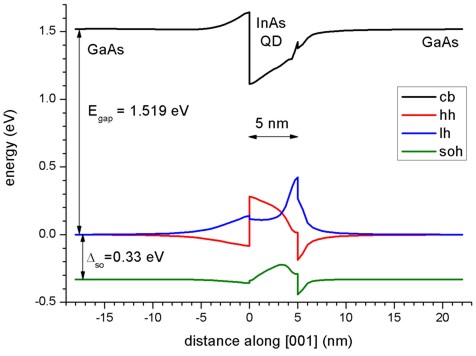
Figure 2.4.8.24 Calculated band edge profile along z axis.
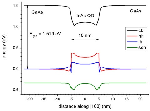
Figure 2.4.8.25 Calculated band edge profile along x axis.
The figures compare well with Figs. 2(a) and 2(b) of [Pryor1998]. However, there are some differences: Due to valence band mixing of the states in the k.p Hamiltonian, we do not have pure heavy and light hole eigenstates anymore. Thus there is some arbitrariness to assign the labels “heavy” and “light” to the relevant eigenstates h1 and h2. Obviously, when solving the full 6-band or 8-band k.p Hamiltonian, this labelling becomes irrelevant because all three hole band edges enter the Hamiltonian simultaneously (in contrast to a single-band effective mass approach where only individual “heavy” hole or “light” hole band edges would be considered).
Electron wave function of the ground state (single-band effective-mass approximation)
Figure 2.4.8.26 shows the probability distribution of the electron ground state (The data is contained in bias_00000\Quantum\probability_shift_dot_Gamma_0001.avs.fld)
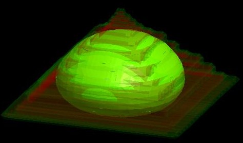
Figure 2.4.8.26 \(\Psi^2\) of the electron ground state inside the quantum dot.
Note
The following sections are preliminary and yet to be updated.
10 nm quantum dot
(Note: Pryor’s Fig. 7 shows the energies for a 14 nm quantum dot). The band gap is 1.519 eV.
Electron energies
(i)   effective mass (me = 0.023 m0) => 0.7000983 eV (only one confined electron state)
(ii)  effective mass (me = 0.04   m0) =>  eV
(iii) effective mass (me(r) = ...   m0) => not implemented in nextnano³
(iv) 8-band k.p                =>  eV
Hole energies
( )   effective mass (mhh = 0.41 m0) => hh1 = -0.585198481 eV
                                     => hh1 = -0.61776 eV
                                     => hh1 = -0.62275 eV
(i)   6-band k.p                => 1.0081402 eV (?) (bad eigenvalues using 6-band k.p with finite-differences)
(ii)  8-band k.p                =>  eV
Transition energy electron - hole
- (i) - ( ): exciton correction 2.9 meV (Pryor: 27 meV)
E_ex [eV]   E_el - E_hl   E_el0 - E_hl0   Delta_Ex     REAL(inter_matV(1))
1.28238     1.27958       1.28530         0.00291947   0.428169
14 nm quantum dot (Pryor’s Fig. 7)
(i)   effective mass (me = 0.023 m0) => 0.6458949 eV (only one confined electron state) + (1.519 - 0.752916) eV = 1.412 eV (in substrate layer below QD)
(i)   effective mass (me = 0.023 m0) => 0.6458949 eV (only one confined electron state) + (1.519 - 0.765522) eV = 1.399 eV (in substrate layer at corner)
(i)   effective mass (me = 0.04   m0) => 0.6248762 eV (only one confined electron state) + (1.519 - 0.765522) eV = 1.378 eV (in substrate layer at corner

14 nm, 6x6k.p, box, nonsym:
-0.56607270
-0.58734305
-0.59621434
-0.60757551
-0.62802221
-0.63650764
Last update: nn/nn/nnnn