Depletion of electrons in a two-dimensional electron gas (2DEG)
In this tutorial you will learn how to setup an input file to simulate the electrostatic potential and the density of electrons in a 2DEG formed at the interface of a GaAs/AlGaAs layers.
Structure simulated
Figure 2.4.13.1 and Figure 2.4.13.2 present the simulated structure, where a two-dimensional electron gas is formed at the interface of the AlGaAs and GaAs (the substrate) materials. Doping the AlGaAs with n-type impurities at a certain distance of this interface improves the confinement of electrons in the 2DEG region. A GaAs layer over the n-AlGaAs region acts as a cap of the device. Finally metallic gates with different geometries are directly deposited on the top of surface.
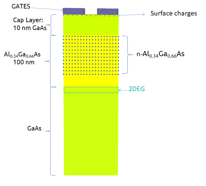
Figure 2.4.13.1 Schematics of a side view of the simulated device
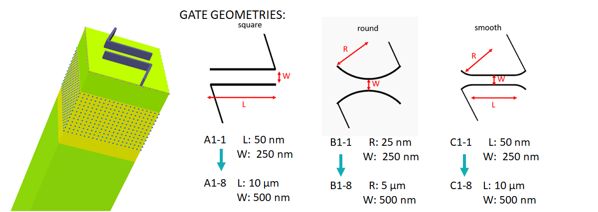
Figure 2.4.13.2 3-dimensional schematics of the simulated structure and typical shapes of gates
In the scope of the project, the density and mobility of electrons in the 2DEG were measured at low temperatures, which were used in the calibration of the structure, in order to estimate the surface charge concentration at the interface of the cap layer and the surrounding environment (air). Additionally, the calibration also assists in the reduction of the incertainty of the doping concentration of the AlGaAs layer.
The methodology of combining simulations and experimental data was developed in the UltraFastNano project that can be found in the papers: E. Chatzikyriakou et al., Unveiling the charge distribution of a GaAs-based nanoelectronic device A large experimental data-set approach, arXiv preprint arXiv:2205.00846, 2022 and H. Edlbauer et al., Semiconductor-based electron flying qubits: review on recent progress accelerated by numerical modelling (link)
Input files
The bias applied to the gates that depletes the electrons in the 2DEG (the pinch-off voltage) is powerful information that can be used to implement the building blocks of Electron Flying Qubits.
A simple method to define this voltage is by simulation of the same device for different voltages applied symmetric to the gates and to observe the value of the bias that depletes the carriers in some specific point of the 2DEG region (here, the center of the structure). The next two files can be used as an example how to set up the structure and all necessary variables for a self-consistent solution of Schrödinger and Poisson equations for performing 2D and 3D simulations.
Input files:
QPC_1D_nnp.in
QPC_2D_nnp.in (uniform grid of 0.25 nm)
QPC_3D_nnp.in (nonuniform grid)
Using nextnanopy or the “Template” feature of nextnanomat input files can be automatically modified and executed. Also it is very helpful to define slices and 2D sections of the 2DEG region in the input file: this is a powerful tool for easy analysis of the data.
1D simulations
It is always a good strategy starting simulations in only one dimension in order to understand how the band edge of the conduction and valence bands influence the most important mechanisms under study. The 1D version of the input file is suitable for simulating the density of carriers in the 2DEG region, when a metallic layer deposited over the whole surface is biased at different voltages. This input file can also be used for calibration of the wafer when, for example, the density of electrons in the 2DEG is obtained experimentally.
2D Simulations
Before simulating 3D devices, that usually requires a large runtime to compute all relevant fields in the structure, it is always recommended starting modelling in only one or two, when possible.
In this specific example, 2D simulations can be used to tune the most important parameters of the physical model in order to reproduce, at least, the qualitative behavior of the experimental data.
The first animation (Figure 2.4.13.3) corresponds to the results of a 2D simulation of the device at the left in Figure1. It illustrates that the free electrons are confined in the 2DEG region and its density decreases as a negative bias \(V_{gate}\) is applied to both gates.
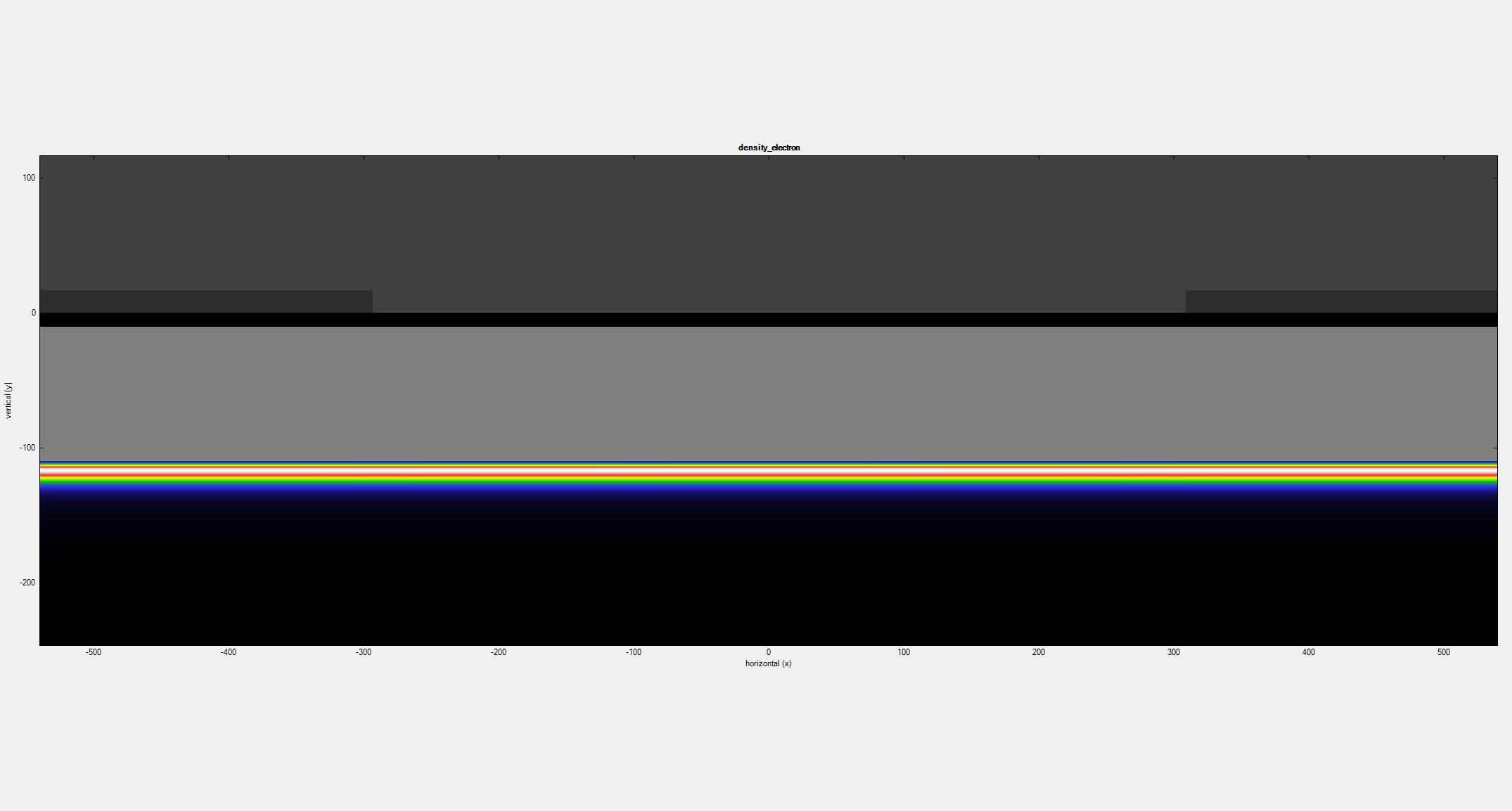
Figure 2.4.13.3 Density of electrons resulting from a 2D simulation as a negative bias is applied to the gates
A slice of the conduction band at the mid-distance between the gates across the growth direction is displayed in Figure 2.4.13.4. The results correspond to the cases where a 0, -1.00, -1.20 and -1.30 V bias is applied to the gates. Overlayed to theses plots, the density of electrons (dashed lines) show that the confinement of carriers at the 2DEG region actually occurs in the 2DEG and a depletion of carriers at this point is expected when very negative value of \(V_{gate}\) is applied to the device.
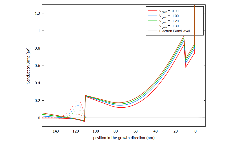
Figure 2.4.13.4 Conduction band (solid lines) and density of electrons (dashed lines) resulting for a 2D simulation as function of the applied bias to the gate. This plot corresponds to the results at the mid-distance of the gates across the growth direction.
3D Simulations
As mentioned before, 2D simulations can be very helpful for a first modeling of the device, and help to reduce the runtime. As shown before they are capable to reproduce the values of the pinch-off voltages for the case when the distance between the gates (W) are very small compared with their lengths (L).
Nevertheless in the most general case, 3D simulations can be required for more accurate estimation of the pinch-off voltage. Additionally, in the development of an Electron Flying Qubit building block computation of the conduction band through the whole device is necessary, in order to reproduce the transport phenomena in the 2DEG layer.
As the simulation time depends on the number of the nodes on the grid, for more complex forms and for large devices (of order of microns) with required fine grid ( of order of nm ), some computers might not have enough memory for the numerical solution of a self-consistent calculation of the Schrödinger and Poisson equations, with a minimum number of wave functions required for such operation.
In this case, a new algorithm was developed within nextnano++ that decomposes the 3D-problem in multiple 1D-problems. In this example, the Schrödinger-Poisson system is solved along the growth direction independently for each pair of coordinates of the nodes of the corresponding perpendicular plane. This decomposition method can be perfect applied to this structure because it is expected that the electrostatic potential does not present any abrupt variation in the any plane perpendicular to the quantization direction. For the application of this algorithm is only required to include the line quantize_x{}, quantize_y{} or quantize_z{} in the quantum section of the input file. In this tutorial the quantum calculations are decomposed in solutions over the growth direction (the z-axis) and, therefore, we use quantize_z{}.
Figure 2.4.13.5 presents an animation of the density of electrons obtained from 3D simulations at 111 nm under the surface (in the 2DEG region) as a function of the applied bias for gates with more complex geometry (square in Figure 1). Slices of this plot for the plane passing between both gates (y=0) can be specified in the input file and are very convenient for automatic extraction of the value where the depletion of electrons occurs. Figure 2.4.13.6 and Figure 2.4.13.7 show that in this case, the pinch-off voltage \(V_{gate}\) is around -1.20 and 1.30 V.
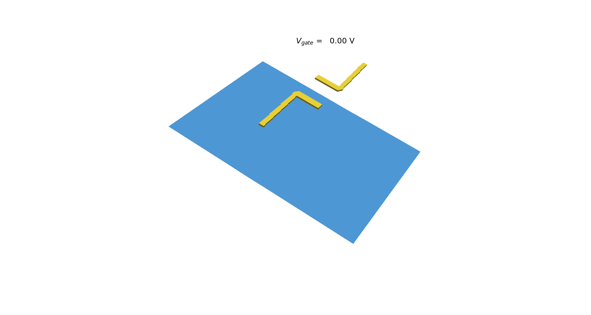
Figure 2.4.13.5 Density of electrons resulting from a 2D simulation as a negative bias is applied to the gates
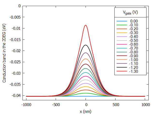
Figure 2.4.13.6 Slice of the computed conduction band in the 2DEG region at 111 nm under the surface as function of the applied bias to the gate. From the image the pinch-off voltage occurs around -1.30 and -1.20 V.
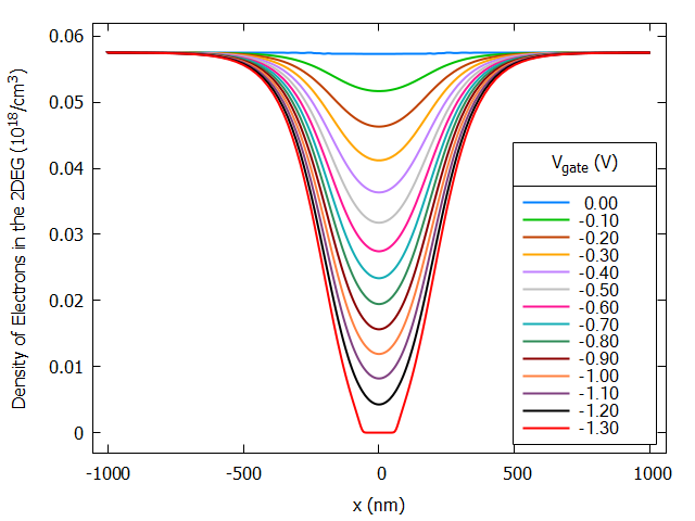
Figure 2.4.13.7 Slice of the computed density of electrons in the 2DEG region at 111 nm under the surface as function of the applied bias to the gate. From the image the pinch-off voltage occurs around -1.30 and -1.20 V.
From an iterative process, accurate values of pinch-off can be extracted from 3D simulations as detailed in the paper from Chatzikyriakou et al. mentioned above, that we strongly recommend to be used.
- Acknowledgment
This tutorial is based on the nextnano GmbH collaboration in the scope of the UltraFastNano Project aiming at development of the first Flying Electron Qubit at the picosecond scale, and it is funded by the European Union’s Horizon 2020 research and innovation program under grant agreement No 862683.

Last update: nn/nn/nnnn