— DEV — I–V characteristic of GaAs p–n junction | 1D/2D/3D
Warning
This tutorial is under construction
- Input Files:
pn_junction_GaAs_ForwardBias_1D_nnp.in
pn_junction_GaAs_ForwardBias_2D_nnp.in
pn_junction_GaAs_ForwardBias_3D_nnp.in
- Scope:
This tutorial shows how to perform bias sweeps to compute IV curves.
- Most relevant keywords:
contacts{ ohmic{ bias steps } }
- Output Files:
IV_characteristics.dat
Introduction
In the present tutorial we are concerned with the question of how to determine the I-V characteristics of a device. For this purpose, one side of the device is biased, and the simulation is repeatedly executed for a range of different voltages. The nextnano++ tool offers a convenient way to perform this bias sweep. The computed current and voltage values are automatically collected in one file. In what follows, we simulate a simple p-n junction (see also p-n junction tutorial), to demonstrate the usage of the keywords which are relevant to trigger the bias sweep.
Input File
First, two contact regions at both ends of the structure are needed: one as source and the other as drain channel. The contact regions will allow us to bias the structure by applying an explicit voltage to either side of the device.
structure{

    ...

    region{
        line{ x = [ -$BOUNDARY, -$SIZE] }   # contact on left device boundary
        contact{ name = leftgate }          # contact name
    }
    region{
        line{ x =[ $SIZE, $BOUNDARY] }      # contact on right device boundary
        contact{ name = rightgate }         # contact name
    }

    ...
}
The actual properties of the contacts are specified inside the group contacts{ }.
There are several contact types available (e.g. ohmic{}, schottky{}, fermi{}, …), each imply
different boundary conditions which are applied to the electrostatic potential \(\phi(x)\).
In our case we choose ohmic{} contacts.
The voltage on the right side is set to zero (bias = 0 V) and the left contact is biased. In order to sweep over different voltages automatically, the bias for the left contact is to be specified as a vector with start and end value (bias = [\(\mathrm{V_{start}}\), \(\mathrm{V_{end}}\)]). The attribute steps specifies the total number of voltage values.
contacts{
    ohmic{ # left contact
        name = leftgate                 # refer to region labeled 'leftgate'
        bias = [ 0 , 1.0]               # [V] start and end value of bias sweep
        steps = 20                      # number of sweep values
    }
    ohmic{ # right contact
        name = rightgate                # refer to region labeled 'rightgate'
        bias = 0.0                      # [V] unbiased
    }
}
For simulating charge carrier transport the Poisson and Current equation are solved self consistently.
It is important to use proper convergence parameter inside the group run{ }.
Note
It is important to be aware that applying different voltages change the physical properties of the system, e.g. the electric field, and therefore it is not guaranteed that one set of convergence parameters are applicable to all voltages of the sweep.
poisson{
    charge_neutral{}                          # initialize Fermi levels in the contacts that charge neutrality is obtained

    # output settings
    output_potential{}
    output_electric_field{}
}

currents{
    mobility_model = minimos                  # mobility model
    recombination_model{                      # recombination model
        SRH       = yes
        Auger     = yes
        radiative = yes
    }
    minimum_density = $MINIMUMDENSITY         # convergence parameter
    maximum_density = 1e14                    # convergence parameter

    # output settings
    output_currents{ }
    output_mobilities{}
    output_recombination{}
}

run{
    current_poisson{
        iterations           = 1000      # max iteration
        current_repetitions  = 10        # current repetition
        alpha_fermi          = 0.7       # under-relaxation parameter
        residual_fermi       = 1e-12     # desired residual of Fermi levels
        output_log           = yes       # information about convergence behavior
    }
}
Results
When the input file is executed, simulation results for each bias value are written in separate folders. These are located in the output folder of the simulation under \bias_xxxxx and contain e.g. band edges, electric fields, convergence behaviors, etc.
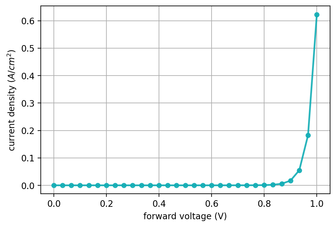
Figure 2.4.3.1 Current density as function of applied bias (1d simulation)
The output folder also contains a file with the combined current-voltage values. The corresponding file is labeled IV_characteristics.dat. The I-V curve, as presented in Figure 2.4.3.1, can be directly visualized in nextnanomat.
- Input Files for nextnano³:
pn_junction_GaAs_1D_ForwardBias_nn3.in
Last update: nn/nn/nnnn