I–V characteristics of ultrathin-body Double Gate Metal Oxide Semiconductor Field Effect Transistor (DG MOSFET)
Attention
This tutorial is under construction
- Input files:
IV_DG-MOSFET_Si_2D_classical_nnp.in
IV_DG-MOSFET_Si_2D_quantum_nnp.in
IV_DG-MOSFET_Si_3D_classical_nnp.in
- Scope:
This tutorial aims to simulate the I-V characteristics of a Double Gate metal oxide semiconductor field effect transistor (MOSFET).
- Output files:
bias_xxxxx\density_electron.avs.fld
IV_characteristics.dat
Double Gate MOSFET
The main idea of a Double Gate MOSFET is to control the Si channel very efficiently by choosing the Si channel width to be very small and by applying a gate contact to both sides of the channel. This concept helps to suppress short channel effects and leads to higher currents as compared with a MOSFET having only one gate.
The geometry of the simulated Double Gate MOSFET structure is shown in Figure 2.5.1.57. The width of the Si channel is 2 nm. The distance between the two gates is 6 nm, i.e. the isolating \(\mathrm{SiO}_2\) is 2 nm thick on each side. The width of the two gates is 20 nm. The distance between source and drain is 60 nm. The widths and the lengths of source, drain, left and right doped source regions are 10 nm x 10 nm each. The length of the 2 nm Si channel (without the square doped source and drain regions) is 40 nm.
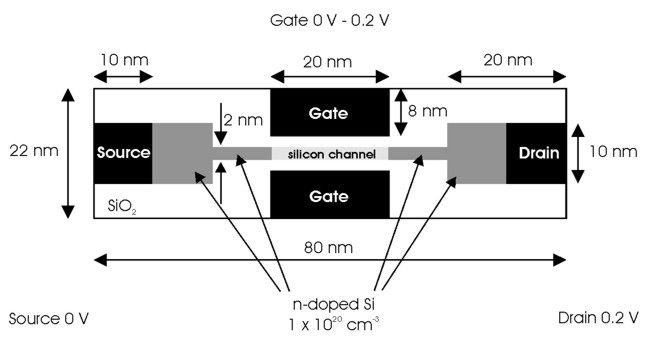
Figure 2.5.1.57 Geometry of the simulated Double Gate MOSFET.
The material regions defined in the input file for the nextnano++ simulations are shown in Figure 2.5.1.58. The blue squares (Si) are n-doped with a concentration of \(1\cdot 10^{20}\,\mathrm{cm^{-3}}\). The 2 nm channel is n-doped with the same concentration from 20 nm to 30 nm and from 50 nm to 60 nm.
A constant bias of 0.0 V and 0.2 V is applied to source and drain, respectively. At the two gates we apply Schottky barriers of 3.443 eV, and sweep over the applied bias from \(0\,\mathrm{V}\) to \(1\,\mathrm{V}\).
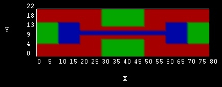
Figure 2.5.1.58 Schematic top view of the material regions defined in the nextnano++ simulations.
The numerical grid employed in the simulations is shown in Figure 2.5.1.59.
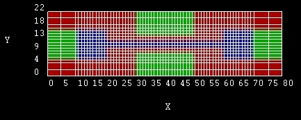
Figure 2.5.1.59 Grid lines of the Double Gate MOSFET
Input file
For the simulations, the following parameters, which are specified in the corresponding input file IV_DG-MOSFET_Si_2D_classical_nnp.in, are used:
The lattice temperature is taken to be 300 Kelvin.
The classical current and nonlinear Poisson equations are solved self-consistently without including the effect of strain.
A two-dimensional simulation is performed. The overall simulation domain, that is the real space region in which the device is defined, is taken to be a rectangle having the size 22 nm x 80 nm.
Electron densities
In Figure 2.5.1.60 the electron density inside the MOSFET structure at \(0\,\mathrm{V}\) is shown. The corresponding data is contained in the file bias_00000\density_electron.avs.fld.
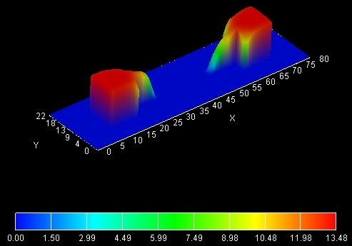
Figure 2.5.1.60 Electron density in units of \(1 \cdot 10^{18}\mathrm{cm^{-3}}\) at \(0\,\mathrm{V}\) gate voltage.
In Figure 2.5.1.61 the electron density inside the MOSFET structure at \(0.2\,\mathrm{V}\) is shown. The corresponding data is contained in the file bias_00002\density_electron.avs.fld. One can clearly see that the electron density has the highest values at the \(\mathrm{Si}-\mathrm{SiO}_2\) interfaces.
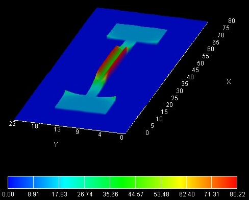
Figure 2.5.1.61 Electron density in units of \(1 \cdot 10^{18}\mathrm{cm^{-3}}\) at \(0.2\,\mathrm{V}\) gate voltage.
For comparison, Figure 2.5.1.61 shows the quantum mechanical electron density inside the MOSFET structure at \(0.2\,\mathrm{V}\). The corresponding input which includes the quantum mechanical computation of the charge density is IV_DG-MOSFET_Si_2D_quantum_nnp.in. One can clearly see that the electron density has the highest values in the middle of the channel and not at the \(\mathrm{Si}-\mathrm{SiO}_2\) interfaces. This is because the wave functions tend to zero at the \(\mathrm{Si}-\mathrm{SiO}_2\) interfaces. The peak values in the source and drain regions are due to classical densities because the quantum region did not extend over the whole source and drain regions.
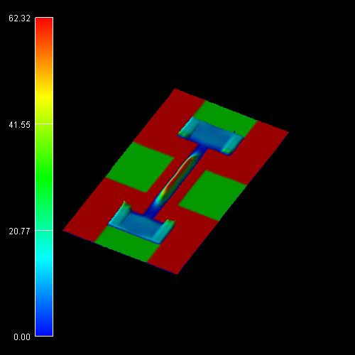
Figure 2.5.1.62 Quantum mechanical electron density in units of \(1 \cdot 10^{18}\mathrm{cm^{-3}}\) at \(0.2\,\mathrm{V}\) gate voltage.
I-V characteristics
In order to test the implementation of the three-dimensional drift-diffusion current, we performed a three-dimensional simulation of the Double Gate MOSFET. The corresponding input file is IV_DG-MOSFET_Si_3D_classical_nnp, where we assume complete ionization of the doping atoms. We further assume that the structure is homogeneous along the \(z\)-direction and assume the \(z\)-direction to be 10 nm long with grid spacing of 2 nm. The calculated current values in units of [A] can be found in IV_characteristics.dat. The current has to be divided by the length of the device along the \(z\)-direction, i.e. by 10 nm, in order to obtain it in units of [A/m]. Figure 2.5.1.63 confirms that the 3D results are in agreement with the 2D results.
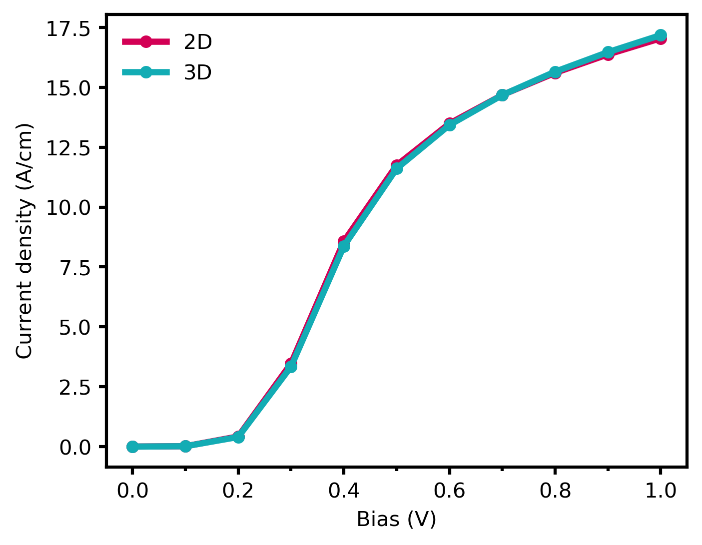
Figure 2.5.1.63 Comparison of the current-voltage characteristics between 2D and 3D simulations.
Last update: nn/nn/nnnn