Conductance of a quantum point contact (gated two-dimensional electron gas)
Attention
A tutorial on computing the conductance using CBR method can be found here
- Related Files:
3D_conductance_in_top_gated_2DEG_nnp.in - simulation of the potential in 2DEG
3D_conductance_in_top_gated_2DEG.py - generates all plots
3D_conductance_in_top_gated_2DEG_verification.py - does not generate conductance
3D_conductance_in_top_gated_2DEG_without_plot.py - generates only conductance
3D_conductance_in_top_gated_2DEG_exercise.py - semiclassical and quantum calculations (exercise)
3D_conductance_in_top_gated_2DEG.ipynb - Jupyter Notebook for practicing the tutorial
The Python scripts and the Jupyter Notebook file are available on our GitHub
- Scope of the tutorial:
computing electrostatic potential using nextnano++
interfacing nextnano++ with Kwant, for computing the conductance between two leads
- Main adjustable parameters in the input file:
calculation with or without Schrödinger -
$solve_quantumdepth of the slice of the 2DEG region -
$slice_in_2DEG(see lines 76 and 77)the widths of the gates -
$gate_widththe gap beetween the gates -
$gap_lengthlowest bias on the top gate -
$top_gate_bias_minhighest bias on the top gate -
$top_gate_bias_maxnumber os bias sweeps of the top gate -
$top_gate_stepsbias of the bottom gate -
$bottom_gate_bias- Relevant output files:
bias_xxxxx\bandedges_2d_2deg_slice.fld (potential energy profile - semiclassical case)
bias_xxxxx\Quantum\energy_subbands_quantum_region_Gamma_2d_2deg_slice.fld (potential energy profile - self-consistent quantum case)
bias_xxxxx\density_electron_1d_section_line_x_center.dat (density of electrons in the growth direction)
Simulated Structure
Figure 2.4.14.28 presents the simulated structure, where a two-dimensional electron gas (2DEG) is formed at the interface of the AlGaAs and GaAs (the substrate) materials. The electron density in the 2DEG is enhanced by doping the region of the AlGaAs with n-type impurities only in the part close to the surface.
A GaAs layer over the n-AlGaAs region acts simply as a cap of the device. On the top of the surface metallic gates are deposited and can present different geometries. We will choose the gates in the Figure 2.4.14.29 as QPCs, to which negative bias will be applied in order to deplete electrons at the center of the 2DEG region. Although these gates pursue one of the simplest geometries, the method here described can also be used for gates with more complex shapes.
The dopant and surface charges concentrations used in this simulation are realistic, and were obtained by the calibration method described in [Chatzikyriakou_PhysRevResearch_2022]
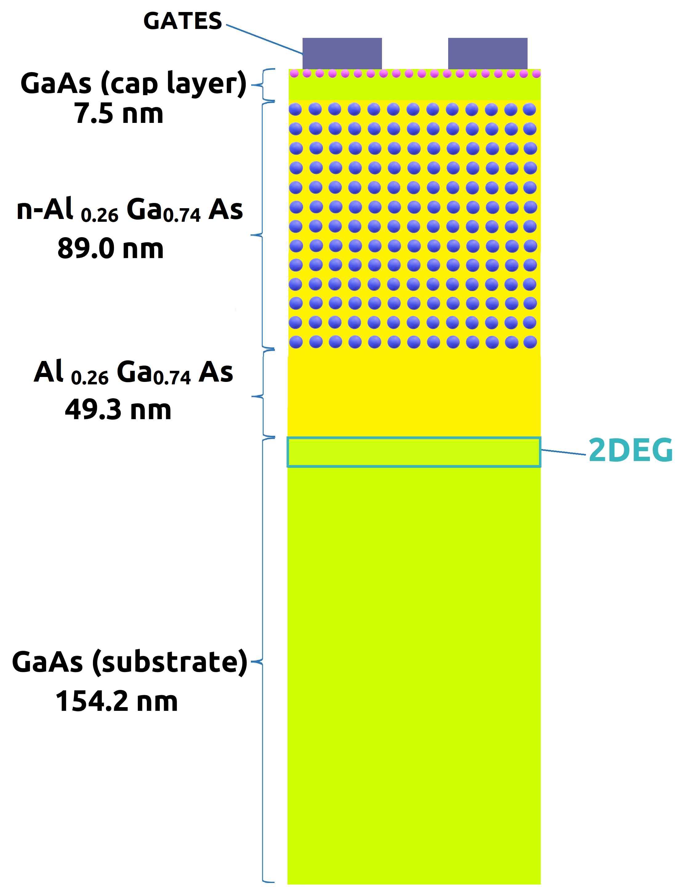
Figure 2.4.14.28 Schematics of a side view of the simulated device
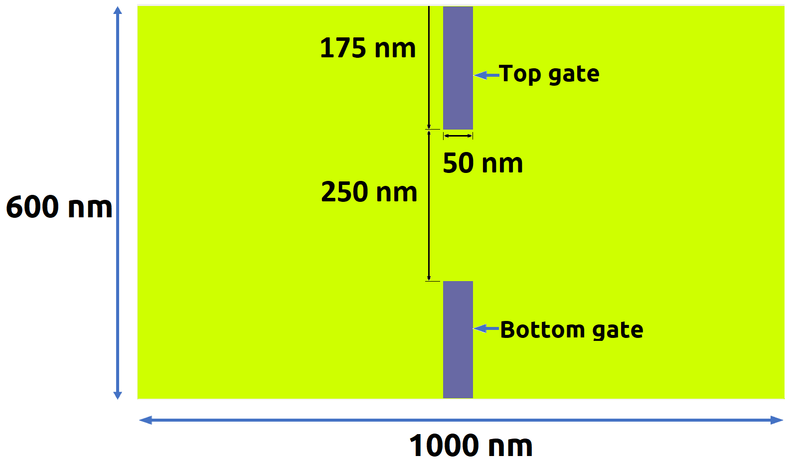
Figure 2.4.14.29 Top view of the gates deposited on the top of the simulations
The Simulation
The main objective of this tutorial is to simulate the conductance between two leads in the 2DEG region as a function of the applied bias in the gates deposited at the top of the structure.
Initially we will use nextnano++ to obtain the conduction band in the device changing the applied bias to the top gate in the range of -1.5 V and 0.0 V. The applied bias to the bottom gate will be kept constant (-1.1V), through the whole set of simulations. For this first phase of this tutorial, we will use the input file: 3D_conductance_in_top_gated_2DEG_nnp.in.
In order to obtain the trasmission coefficients between two leads in the 2DEG, we will import a slice of the conduction band in this region into the software Kwant, using the Python script: 3D_conductance_in_top_gated_2DEG.py
Kwant is an open-source tool that performs numerical calculations on tight-binding models. For the installation of Kwant in your computer, please, follow the instructions on the Kwant webpage.
Phase 1: Obtaining the conduction band in the 2DEG region using nextnano++
The conduction band in the whole device can be obtained as a solution of the 3D-Poisson equation.
For realistic devices, a large number of nodes in the grid is required to evaluate with high accuracy the voltage that depletes electrons at the center of the 2DEG region. The nextnano++ input file sweeps automatically the value of the top gate (\(V_{gate}\)) and generates 2D-slices of the band edges in the 2DEG plane that will be used in the next phase of the simulation.
Phase 2: Setting up Kwant
In order to setup Kwant in a consistent way with the configuration of nextnano++ we need to define the next variables:
the effective mass of electrons in the 2DEG region
ms = 0.067 * 9.109e-31lattice constant of the tight-binding system (nm)
a = 1conversion constant from eV (output of nextnano++) to Kwant energy unit
T = hbar*hbar/2/nm/nm/ms/e
where:
e = 1.602e-19is the electron charge (in C),
hbar = 6.626e-34/2/np.piis the Dirac constant (in Js),
h = 6.626e-34is the Planck constant (in Js),
nm = 1e-9is the conversion factor from 1 nanometer to 1 meter (in m),
Additionally, it is convenient to define a smaller portion of the slice of the potential obtained in the previous phase as the scattering region that will be used by Kwant. Here we will use a square scattering region with size of 400 nm x 400 nm, with the same center as before, the coordinates (0,0).
Phase 3: Computing the conductance coefficients with Kwant
Describing briefly the Kwant script 3D_conductance_in_top_gated_2DEG.py, the program reads the file containing the potential in the 2DEG region ( a 2D-slice at a depth of -146.8 nm under the surface ), whose path is specified in the script through the variable path_extracted_potential. Through interpolation, Kwant maps the values of the potential into each node of the corresponding 2D-square lattice defined in the previous phase.
This is the basic element for building the system of equations to be solved under the tight-binding approach, whose the matrix elements and hoppings are set by discretization of the Hamiltonian:
where \(V(x,y)\) is the potential extracted from nextnano++. In this initial calculation we will start simulating the potential without computing Schrödinger equation.
The leads will be considered as ohmic contacts, and are attached to the left (lead 0) and to the right (lead 1) of the scattering region, as shown in Figure 2.4.14.30.
At this point it is convenient to verify the band edges of both leads, one of them plotted in the Figure 2.4.14.30. Finally the program solves the system of equations and the conductance from lead 0 to lead 1 is computed, for the especific potential imported. As example, when applying a voltage of -1.11 V to the upper gate of the structure, and -1.1 the the lower gate, the conductance between the two leads in the 2DEG is equal to 2.0074 \(2e^2/h\)
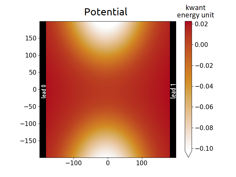
Figure 2.4.14.30 Imported conduction band when a bias of -1.11V is applied to the top gate.
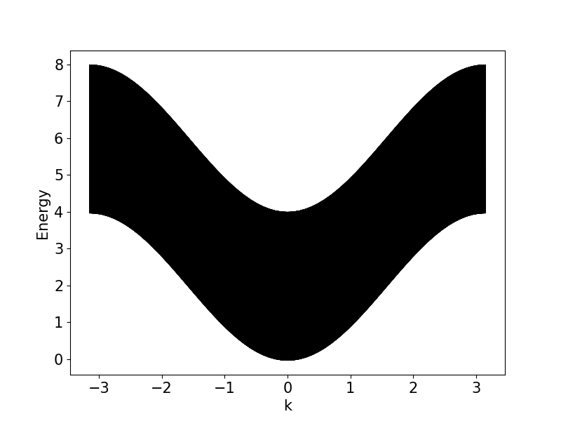
Figure 2.4.14.31 Band structure of the lead 0 for top gate voltage equal to -1.11 V.
As we mentioned before, QPCs can be a very useful structure to control the conductance of electrons in a 2DEG region. In this example, we can verify how changes on the bias of one of the gates modifies the transport of electrons in the 2DEG region.
The Kwant script iteratively will import each potential simulated in nextnano GmbH and compute the correspondent conductance. This script requires that you have nextnanopy installed in your machine, that can be downloaded for free in our
nextnanopy repository. In the script it will be required to modify variable path_extracted_potential with the path where the simulation results of nextnano++ will be stored. As this process will process 101 files, it could take some minutes to perform the calculations. At the end of the process, a plot will be generated in your screen.
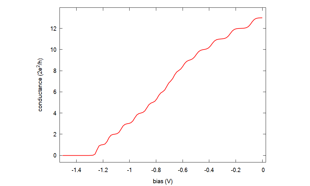
Figure 2.4.14.32 Conductance between lead 0 to lead 1 as function of the bias applied to the top gate
The Figure 2.4.14.32 presents the channel conductance computed for each value of \(V_{gate}\). The steps in the curve show the expected quantization for this device.
Phase 4: Computing conductance with potential from self-consistent Schrödinger-Poisson calculations
Until this point our potential has considered only the solutions of the Poisson equation for evaluation of the density of electrons in the 2DEG region. Nevertheless, it is expected that the density of states of the semiclassical potential be substantially different from the case when quantum effects are taken into account, especially at low energies.
Figure 2.4.14.33 presents the density distribution in the growth direction (perpendicular to the 2DEG plane) at the center of device ( \(x = 0\) nm and \(y = 0\))for \(V_{gate} = -1.17 V\). They correspond to the results from nextnano++ simulations with and without quantum calculations.
First we observe that both distributions present their maxima at different depths of the 2DEG. This result is expected because the confined states are discrete and present their maxima not so close to the interface. The integration of the density of states over a triangular-shaped potential for the semiclassical case generates distributions closer to the deepest part of the potential ( close to the interface ) when compared with the case including quantization.

Figure 2.4.14.33 Density of electrons in the growth direction at the center of the device ( \(y = 0\) nm and \(z = 0\)) for \(V_{gate} = -1.17 V\) for semiclassical computation (without quantization) and for self-consistent Schrödinger-Poisson calculations (with quantization)
Last but not least, we can observe that the peak of the electron distribution for the same value of \(V_{gate}\) is higher when quantum solution is not taken into account. This practically means that for the semiclassical solution it is required to apply more negative bias in order to deplete electrons that are accumulated close to the interface. In another words, it is expected that neglecting quantum effects the depletion of the electrons show occur at higher values than predicted from the semiclassical approach.
In order to analyse the impact of including quantum effects in the conductance calculations we need to import the final results from nextnano++ values of the eigenstate of the ground state (E1) from the file energy_subbands_quantum_region_Gamma_2d_2deg_slice.fld in the Quantum folder. The imported potentials used both cases ( with and without quantization) were obtained for a 2D-slice 161.8 nm below the surface, where the density of electrons for the quantum solution is maximum.
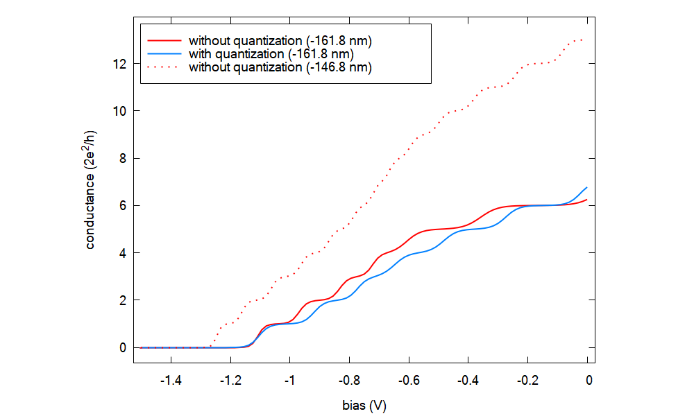
Figure 2.4.14.34 Conductance between lead 0 to lead 1 as function of the bias applied to the top gate at the plane z = 161.8 nm in the 2DEG region with and without quantization along the growth direction ( in solid lines ). In dotted lines the conductance without quantization is shown at the depth where the electron density is higher in the 2DEG ( 146.8 nm below the surface, as shown in Figure 2.4.14.32)
We can observe that at this plane the depletion of electrons in both simulations occurs at the same bias (around -1.11 V), as discussed and predicted above.
As a final conclusion, for accurate determination of the pinch-off voltages, obtaining the potential from self-consistent simulations of Schrödinger-Poisson are required.
- Exercise:
In order to reproduce the figures of the last section, modify and run the nextnano++ input file for both cases:
$solve_quantum = 0and use the option$slice_in_2DEG = 161.8at the line 77 (save the input file with the name 3D_conductance_in_top_gated_2DEG_exercise_nnp.in)
$solve_quantum = 1and use the option$slice_in_2DEG = 161.8at the line 77 (save the input file with the name 3D_conductance_in_top_gated_2DEG_QM_exercise_nnp.in)Edit the path of the output folders of both simulations in the script 3D_conductance_in_top_gated_2DEG_exercise.py (variables
path_extracted_potential_Poissonandpath_extracted_potential_QM), and compute the transmission.- Acknowledgment
This tutorial is a result on the nextnano GmbH collaboration in the scope of the UltraFastNano Project aiming at development of the first Flying Electron Qubit at the picosecond scale, and it is funded by the European Union’s Horizon 2020 research and innovation program under grant agreement No 862683. The tutorial contains part of results from a collaboration of Institut Néel (CNRS), CEA-IRIG and nextnano GmbH Lab in France, and nextnano GmbH in Germany.

Last update: nn/nn/nnnn