Landauer conductance and conductance quantization: from quantum wires to quantum point contacts
Header
- Files for the tutorial located in nextnano++\examples\transmission:
1D_GaAs_conductance_nnp.in - simulations of 1D quantum wire in nextnano++
1D_GaAs_conductance_nn3.in - simulations of 1D quantum wire in nextnano³
2D_transmission_QPC_nnp.in - simulations of QPC in 2DEG
2D_transmission_QPC_potential_of_2DEG_1.fld - numerically obtained energy profile of QPC
2D_transmission_QPC_potential_of_2DEG_2.fld - numerically obtained energy profile of differently shaped QPC
- Main adjustable parameters for 1D simulations (quantum wire):
upper boundary for transmission energy -
%E_maxthe barrier widths -
%Delta_x = %Barrier_max - %Barrier_minthe barrier heights -
%Barrier_Heightthe temperature -
%TemperatureFermi levels of left (xmin_contact < x < x_min) and right (x_max < x < xmax_contact) regions (leads) -
%Fermi_leftand%Fermi_rightthe effective mass of the electron -
%effective_mass
- Relevant output files of 1D simulations (quantum wire):
Results\BandEdges.dat (energy profile)
Results\Transmission_cb_sg1_deg1.dat (transmission)
Results\LocalDOS_sg1_deg1_Lead1.fld and Results\LocalDOS_sg1_deg1_Lead1.fld (LDoS)
Results\IV_characteristics.dat (currents)
- Main adjustable parameters for 2D simulations (QPC):
dimensions of the device -
$x_lengthand$y_lengthgrid spacing in x and y direction,
$grid_spacingnumber of eigenvalues in the device and the leads -
$num_eigenstates_deviceand$num_eigenvalues_leadsthe temperature -
$Temperatureenergy range and resolution that the transmission will be computed -
$E_min,$E_maxand$delta_energypath of the file to be imported -
$pathPotentialFile
- Relevant output files of 2D simulations (QPC):
bias_00000\bandedges.fld (energy profile)
Structure\contact.fld (contacts)
bias_00000\CBR\transmission_sums_device_Gamma.dat (transmission)
Introduction
Conductance, \(G\), is the quantity which describes the relation between an electric current, \(J\), and an applied voltage, \(V_{\rm dc}\), which causes this current. In this tutorial, we briefly review the analitical theory, which allows one to calculate the conductance, and compare it with the numerical approach implemented into the nextnano software. We discuss only the dc case with the main focus on the linear response regime where \(J= G V_{\rm dc}\).
Unlike conductivity, which characterizes properties of a material, conductance describes a given sample. Therefore, geometry and size of the sample matter. We start below from an example of a quantum wire where the electric current is carried either by one (one-dimensional, 1D) or several (quasi-1D) propagating modes. Conductance of the quantum wire is described by the seminal Landauer theory. A simple introduction to the Landauer theory can be found in the book by S. Datta [Datta], section 2 “Conductance from Transmission”.
The setup of the Landauer theory is shown in the upper panel of Figure 2.4.14.7. The device is connected via left and right ideal wires (ballistic conductors) to two leads with different chemical potentials. The current flows from the material with a larger chemical potential to that with a smaller one.
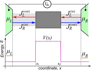
Figure 2.4.14.7 Upper panel: Landauer setup. Left and right leads (green regions) are connected to a semiconductor device (dark gray square) via connecting wires (light gray regions). Lower panel: chemical potentials of the leads (orange lines) and the energy of the potential barrier (magenta lines).
In the standard approach, the leads are two- or three-dimensional large conductors and contacts between the leads and the wires are reflectionless. This ensures that electrons supporting the current \(J_{\rm R}^{\rm (in)}\) are in equilibrium with the left lead and have the chemical potential \(\mu_L\). Similarly, the electrons supporting the current \(J_{\rm L}^{\rm (in)}\) are in equilibrium with the right lead and have the chemical potential \(\mu_R\).
Simulations of the current in 1D wires
Let us assume that all elements of the electric circuit are purely 1D, there is no temperature gradient, and the chemical potentials of the leads are shifted by the applied external voltage, \(\mu_R - \mu_L = e V_{\rm dc}\).
Attention
The value of chemical potentials is not calculated in this tutorial but is set a kind of “artificially”. Of course, this value must be in agreement with physics of a given material. For example, when the temperature (at \(k_B=1\)) is smaller than the energy gap separating the conduction and valence bands, the chemical potential of an intrinsic unbiased semiconductor is close to the center of that gap, see e.g section 3 The Fermi-Dirac Distribution in [Grahn].
Since the connecting wires are ballistic and the contacts are reflectionless, the backscattering of the electrons can occur ony inside the semiconductor device. We model this by including a potential scatterer (a square barrier) into the simulations. Hence, the scattering inside the device is elastic, the energy of the scattered electron is unchanged, and the electrons supporting the currents \(J_{\rm R,L}^{\rm (out)}\) are a mixture of the electrons with the chemical potentials \(\mu_{R,L}\). The energy landscape of the device containing a square potential, \(V(x<x_1)=V(x>x_2)=0, V(x_1<x<x_2)=V_0\), is shown in the lower panel of Figure 2.4.14.7. The electrons whose energy is small, \(E < V_0\), can tunnel through the potential barrier. The electrons with large energies, \(E > v_0\), can be reflected due to quantum effects. For the simple case of the rectangular barrier, the transmission in both cases is known:
Here \(\tilde{k}=\sqrt{2 m |V_0 - E|)|}/\hbar\), \(\kappa = \sqrt{V_0^2 / 4 E | V_0 - E|}\), \(m\) is the (effective) mass of the electron and \(\hbar\) is the Planck constant. Transmission of the device is needed to calculate the current: The total current is the difference of currents flowing in opposite directions: \(J = J_R^{(\rm{in})} - J_L^{(\rm{out})} = J_R^{(\rm{out})} - J_L^{(in)}\). Here, upper indices indicate whether a given current flows into or from the device. The Landauer formula allows one to express \(J\) via \(\cal{T}\). In the purely 1D setup, the current reads:
where \(e\) and \(k\) are the electron charge and its wave-vector, respectively. The electrons in the left/right leads are described by the Fermi-Dirac distribution functions, \(f_{L,R}\). The second equality in (2.4.14.3) has been obtained after changing the integration variable from the electron wave-vector to its energy.
If \(V_0=0\), i.e. \({\cal T}=1\), a simple calculation yields \(J=G_0 V_{\rm dc}\) where \(G_0=2e^2/h\) is the quantum of the conductance. The nextnano software reproduces this result with a very high accuracy, see Figure 2.4.14.8. The numerical simulations presented in this tutorial were done by using Contact Block Reduction method [CBR], see also tutorial on the CBR method.
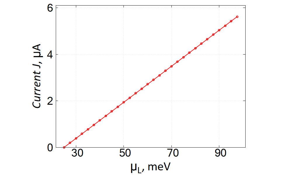
Figure 2.4.14.8 Numerically calculated IV-characteristics of a ballistic 1D conductor, \(V_0=0\). We have chosen GaAs as the material of the conductor with the total length 32 nm at \(\mu_R = 25 {\rm meV}\); the temperature was set to \(T=50 {\rm mK}\). Note that these parameters has no influence on the universal slope of the IV straight line which is equal to \(G_0\). For chosen parameters of the numerical solver and the numerical integration procedure (cf. the sample input file), the difference between the numerically calculated slope and \(G_0\) is \(\simeq 4\%\).
The users of the nextnano software should pay attention that regions, which are called “leads” in the CBR-based sample input files, are actually interfaces between the devices and the connecting wires. These interfaces have minimal width of the space discretization. In the toy model which we discuss the chemical potential of each interface is equal to that of the corresponding lead. Such a simplification of the Landauer setup in natural in the CBR method. One may refer to the interfaces between the device and the connecting wires as “CBR-leads”. An example of the CBR-leads is shown below for the case of the two-dimensional (2D) device.
Figure 2.4.14.9 and Figure 2.4.14.10 shows the transmission and the IV characteristics of the device which contains the square scattering potential of width 30 nm with \(V_0=100 {\rm meV}\).
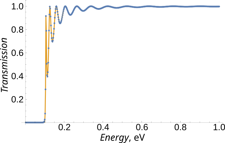
Figure 2.4.14.9 Transmission of a 1D conductor with \(V_0=100 {\rm meV}\) and width 30nm. Orange line and blue dots shows the exact analytical answer, Eqs. (2.4.14.1) and (2.4.14.2), and CBR calculations, respectively.
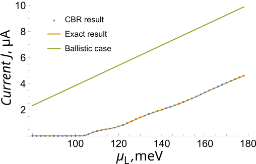
Figure 2.4.14.10 IV-characteristics of a 1D conductor with \(V_0=100 {\rm meV}\) and width 30 nm at \(\mu_R = 50 {\rm meV}\). Other parameters are the same as in Figure 2.4.14.8. Orange line and blue dots shows the exact analytical answer [obtained by using Eqs. (2.4.14.1) and (2.4.14.2)], and CBR calculations. Green line exemlifies the ballistic law \(J = G_0 V_{\rm dc}\).
Since transmission of the device is exponentially small at energies below 0.1 eV, the current become nonzero only at \(\mu_L > 0.1 {\rm eV}\) and, after some transient, the IV characteristics becomes again linear with the slope being close to \(G_0\) with accuracy of several percents.
- Exercise
- Calculate numerically transmission and current through a biased potential which linearly
increases from the value \(V(x_1) = V_1\) to \(V(x_2) = V_2\) with \(V_1 < V2\). Compare the result of simulations with that for the unbiased barrier.
- Repeat the simulations for the inverted biased barrier: \(V(x_1) = V_2\) to \(V(x_2) = V_1\)
keeping all other parameters the same as in the previous task. Do transmission and current change under spatial invertion of the barrier? Explain your answer.
Transmission and conductance of QPC, conductance quantization
The CBR method implemented in nextnano software allows one also to calculate conductance of more complicated semiconductor devices, for example, of a quantum point contact (QPC). QPC in a 2D electron gas (2DEG) can be created in a semiconductor heretostructure by a voltage applied to a top gate. In this case, the potential energy in the plane of the 2DEG can be obtained from the numerical solution of the Poisson equation. An example of such a profile of the potential energy is shown in Figure 2.4.14.11.
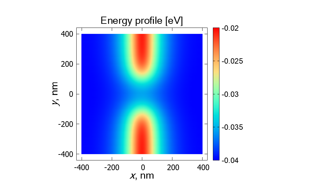
Figure 2.4.14.11 An example of the numerically obtained energy profile for a QPC in the plane of the 2D electron gas. The simulations were done for the 2D electron gas in GaAs at temperature \(100 \rm mK\).
The energy profile can be imported into the nextnano GmbH procedure which calculates transmission, e.g., from left to right boarder of the sample. The left CBR-lead used in this tutorial is illustrated in Figure 2.4.14.12. The right CBR-lead is attached at \(x=400{\rm nm}\).
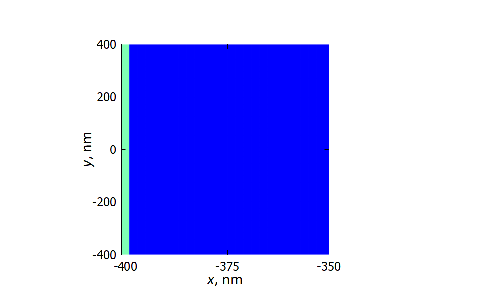
Figure 2.4.14.12 Illustration of how the left CBR-lead (light green region) is attached to the device (blue region). The width of the lead along x-axis is equal to the step of the space discretization. The width of the lead along y-axis has been chosen to be equal to the width of the device.
Numerically calculated energy dependence of the QPC transmission is shown in Figure 2.4.14.13. Temperature corrections to the transmission (due to the temperature-dependent gap) and to the conductance (due to the thermal broadening of the distribution functions) are negligibly small in the sub-Kelvin range (\(\ll 1 \rm K\)) and we neglect them in this tutorial.
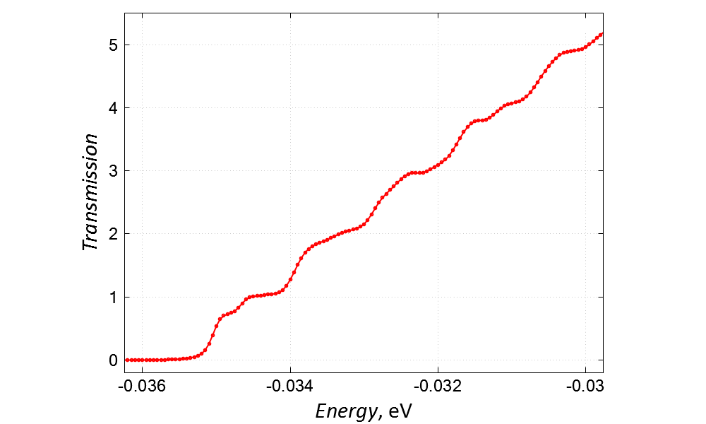
Figure 2.4.14.13 Numerically calculated energy dependence of the transmission via the QPC which is presented in Figure 2.4.14.11. The bottom of the conduction band, \(E_0\), of the gated 2DEG is located at \(\simeq -40{\rm meV}\). Hence, \(E_0\) is the origin of the energy for this example.
The lowest modes with the energy \(< -35{\rm meV}\) are localized near the CBR-leads and do not contribute to transmission. A small plateau of \({\cal T}\simeq 1\) at \(-34.5{\rm meV} < E < -34{\rm meV}\) corresponds to the energies where the first delocalized mode of the device yields its maximum contribution to the transmission. The second (slightly smeared) plateau, \({\cal T}\simeq 2\), signals that the second delocalized mode yields its maximum contribution to the transmission, etc.
The example of the gate-induced QPC is 2D and requires 2D simulations. However, the second equation in (2.4.14.3) still can be used. It suggests that, if temperature and \(V_{\rm dc}\) are extremely small, then linear conductance is proportional to transmission: \(G_{\rm QPC} = G_0 {\cal T}(\mu)\). Negative values of the chemical potential, \(\mu\), of the gated semiconductor structure are related to the choice of the origin, which is explained above. To conclude, we note that plateaux in the energy dependent transmission correspond to those in the conductance which are called in the literature “conductance quantization”.
- Exercises
- The above example was based on the QPC geometry taken from the file 2D_transmission_QPC_2D_potential-v1_of_2DEG.fld.
File 2D_transmission_QPC_2D_potential-v2_of_2DEG.fld contains another QPC geometry which results from a different shape of the top gate electrode. Use this file with the alternated QPC geometry, process it with the help of the nextnano GmbH input file, and calculate the QPC transmission.
Attention
The minimal energy, above which transmission is finite (not zero), depends on the QPC geometry and on the applied gate voltage. Hence, one has to find an appropriate energy range where the plateaux of the quantized conductance are well visible.
Compare the energy profile and the energy dependent transmission for the both shapes of the QPC.
- Note that the second QPC shape does not possess “left \(\leftrightarrow\) right” inversion symmetry (inversion
with respect to the line \(x=0\)). Compare transmissions from the left to right CBR leads with that from the right to left leads. Are they equal? Explain your observation.
Last update: 17/07/2024