Quantum Dot Molecule
In this tutorial, we study two coupled quantum dots (QDs), i.e. two “artificial atoms” that form an “artificial molecule”. The two QDs are asymmetric and differ with respect to their height (4 nm and 6 nm).
With no electric field, the groundstates of both elcectron and hole are localized at the larger QD. By applying the electric field and increasing its strength, the hole groundstate becomes bonding state and then localizes at the smaller QD. At the same time the electron groundstate is still localized at the larger QD because of the weaker coupling between the two QDs due to the heigher barrier height. We will see this leads to the change from an direct exciton to indirect exciton.
The relevant input files are as followings:
3DQD_molecule_cuboid_asymmetric_nn3.in / *_nnp.in
Some of the material parameters that are used in this tutorial are based on the paper of
M. Grundmann, D. BimbergFormation of quantum dots in twofold cleaved edge overgrowthPhys. Rev. B 55 (7), 4054 (1997).
i.e. they are the same as in the 3D CEO QD tutorial (apart from the effective masses).
Simulation
This simulation has the following features:
We keep things simple by using cuboidal shaped GaAs QDs surrounded by Al0.35Ga0.65As barriers, i.e. we neglect strain and piezoelectric effects which is reasonable as the two materials GaAs and Al0.35Ga0.65As have pretty similar lattice constants.
We also neglect the wetting layers and excitonic effects.
In order to keep the CPU time to a minimum, we do not use the k.p approximation, i.e. we use for both electrons and the heavy hole a single-band effective mass approximation for the Schrödinger equation (parabolic and isotropic effective mass tensor). Nevertheless, this is sufficient to show some basic quantum physical effects of this QD molecule.
We use different electron and hole masses in the barrier and well material, respectively.
The left QD has the dimensions 10 nm x 10 nm x 4 nm (smaller dot). The right QD has the dimensions 10 nm x 10 nm x 6 nm (larger dot).
The two QDs are separated by a 2 nm Al0.35Ga0.65As barrier.
The grid resolution is 0.5 nm (rectangular tensor grid). This leads to a 3D Schrödinger matrix of dimension 50,225.
We apply Dirichlet boundary conditions to the Schrödinger equation, i.e. the wave functions are allowed to penetrate the following distances into the barrier material (on each side): - along the x and y directions: 4 nm - along the z direction: 4.5 nm
We vary the electric field along the growth direction (z axis) in steps of -2.5 kV/cm, i.e. from 0 kV/cm to -40 kV/cm.
Results
Electron and heavy hole ground states
The following figures show the square of the electron (left side) and heavy hole (right side) wave functions (isovolumes of 25 % of \(\psi^2\)) for different applied electric fields (0 kV/cm, -17.5 kV/cm, -40 kV/cm). A slice through the conduction and valence band edges along the growth direction through the center of the QDs is also shown.
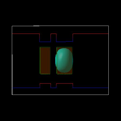
Zero electric field
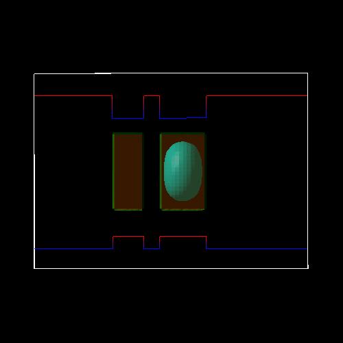
Electric field of -17.5 kV/cm
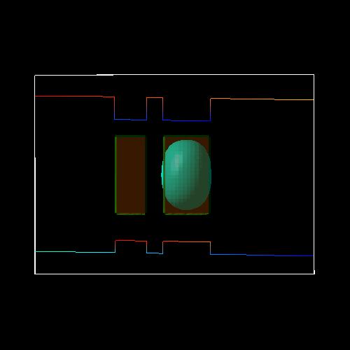
Figure 2.4.8.11 electron ground state for an electric field of -17.5 kV/cm
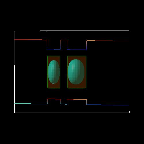
Figure 2.4.8.12 heavy hole ground state for an electric field of -17.5 kV/cm
At an electric field of -17.5 kV/cm, the electron is still located in the larger dot on the right side, whereas the heavy hole forms a bonding (Figure 2.4.8.12) and an antibonding state (not shown) and is thus located in both wells (strong coupling). The exciton that is formed is something in between a direct and an indirect exciton.
Electric field of -40 kV/cm
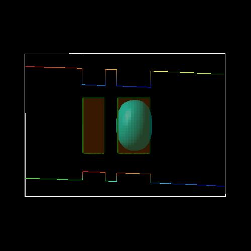
Figure 2.4.8.13 electron ground state for an electric field of -40 kV/cm
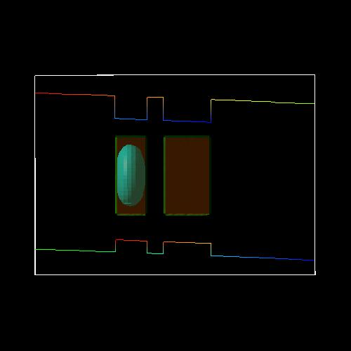
Figure 2.4.8.14 heavy hole ground state for an electric field of -40 kV/cm
At an electric field of -40 kV/cm, the electron is still located in the larger dot on the right side, whereas the heavy hole ground state is now located in the left QD. An indirect (dark) exciton is formed. The exciton is called dark because the electron-hole overlap is much smaller and thus its oscillator strength (probability of optical transition) is much weaker (see Figure 2.4.8.23 below on spatial electron-hole overlap integrals).
Electron and heavy hole energies
Figure 2.4.8.15 shows the electron energies of the ground state (e1) and the first excited electron state (e2) of the QD molecule. The ground state (e1) is always located in the larger QD (right side) whereas the first excited electron state (e2) is always located in the smaller QD (left side). The third and the forth eigenstate (e3, e4) are degenerate (not shown) because our QD molecule has a symmetry with respect to the x and y coordinates. They are always located in the right QD.
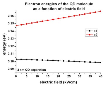
Figure 2.4.8.15 Electron energies
Figure 2.4.8.16 shows the heavy hole energies of the ground state (h1) and the excited hole states (h2, h3, h4, h5) of the QD molecule. In contrast to the electrons, the hole coupling between the two QDs is much stronger due to the smaller barrier height. At -17.5 kV/cm anticrossing between the states occur due to the formation of bonding and antibonding states (see Figure 2.4.8.17 to Figure 2.4.8.21 of the hole wave functions further below).
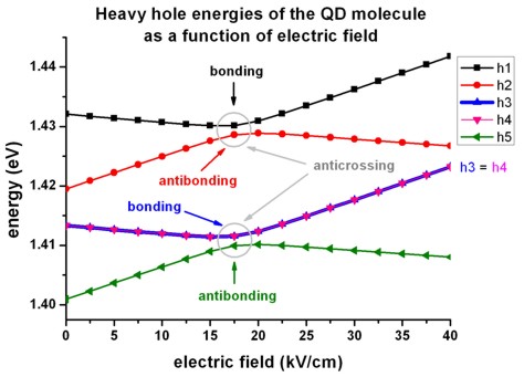
Figure 2.4.8.16 Heavy hole energies
Bonding and antibonding heavy hole state at anticrossing point
The following figures show the square of the lowest five hole wave functions (isovolumes of 2 % of \(\psi^2\)) at an electric field of -17.5 kV/cm.
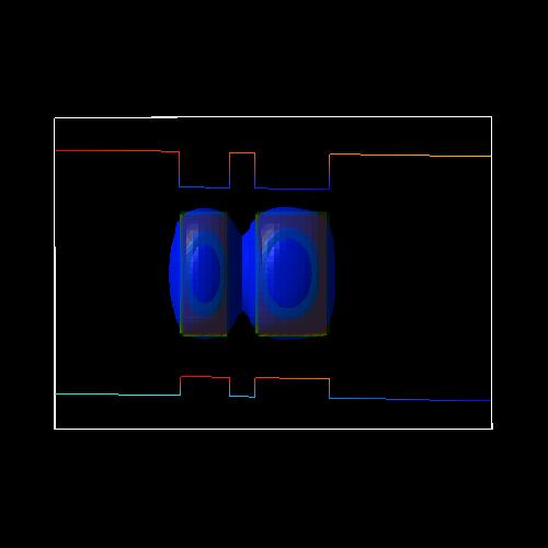
Figure 2.4.8.17 heavy hole (h1) ground state at -17.5 kV/cm (bonding)
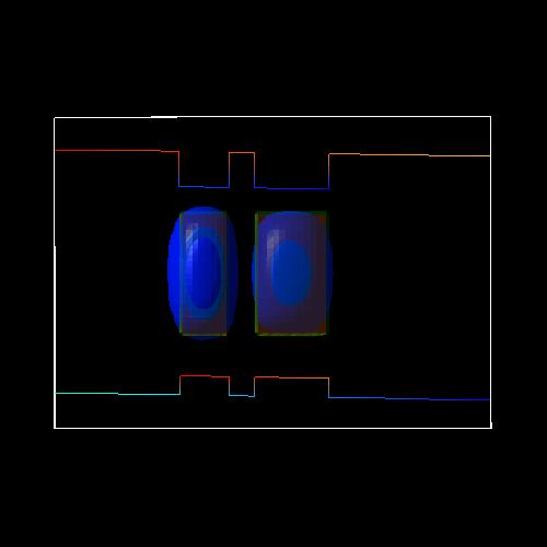
Figure 2.4.8.18 heavy hole (h2) first excited state at -17.5 kV/cm (antibonding)
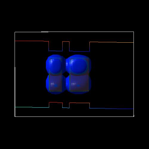
Figure 2.4.8.19 heavy hole (h3) state at -17.5 kV/cm (bonding)
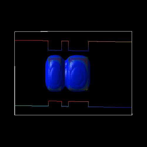
Figure 2.4.8.20 heavy hole (h4) state at -17.5 kV/cm (bonding)
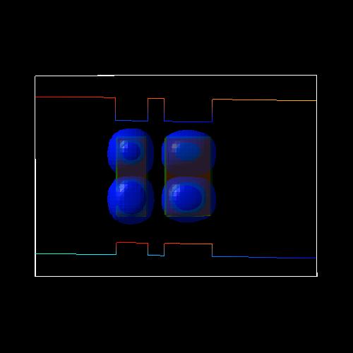
Figure 2.4.8.21 heavy hole (h5) state at -17.5 kV/cm (antibonding)
Electron-hole transition energies
The following figure shows the five lowest electron-hole transition energies of the QD molecule as a function of electric field. For fields smaller than -17.5 kV/cm a direct (bright) exciton is the ground state (both electron and hole wave function are located in the larger QD (right side), whereas for fields larger than -17.5 kV/cm an indirect (dark) exciton is the ground state where the electron is located in the larger QD (right side) and the hole is located in the smaller QD (left side). Therefore, the nature of the QD molecule ground state changes from direct to indirect.
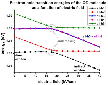
Figure 2.4.8.22 Electron-hole transition energies
Electron-hole overlap
To understand the strength of the optical transitions we have to evaluate the matrix elements of the envelope functions, i.e. the spatial overlap integral over the electron and hole wave functions.
\[\int \psi_{el,i}^*(x)\psi_{hl,j}dx\]
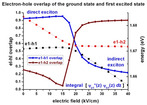
Figure 2.4.8.23 Spatial electron-hole overlap integrals
Last update: nn/nn/nnnn