MOS Capacitor & MOSFET
Section author: Daryoush Nosraty Alamdary
The purpose of this tutorial is to show how the results of our simulation software (which solves the Poisson and drift-diffusion current equations numerically) compare with analytical equations given in standard text books on MOSFETs. The analytical equations use certain approximations and assumptions which limit their applicability. Nevertheless, in most cases the agreement is very good as demonstrated in this tutorial.
Contents
Part 1: Capacitance-voltage characteristics of a 2D MOS capacitor
In the first part of this tutorial we discuss the capacitance-voltage (C-V) characteristics of the MOS capacitor in a 2D simulation. (For a 1D simulation of the C-V characteristics, see also this tutorial: “Capacitance-Voltage curve of a “metal”-insulator-semiconductor (MIS) structure”). Our MOS has the same dimensions and properties (channel length, doping profiles and gate contact type) as the corresponding MOSFET discussed in Part 2.
Part 2: Current-voltage characteristics of a 2D n-Channel MOSFET
In the second part of the tutorial, we start with the design of the MOSFET based on its 2D MOS capacitor, and then discuss its input and output characteristics and their respective conductances, namely transconductance and channel conductance.
Part 3: Mobility models and pinch-off in a 2D n-Channel MOSFET
In this part we discuss and compare the effect of different mobility models on the output characteristics of the MOSFET and how they affect properties such as pinch-off, saturation, etc.
References
[Goetzberger] A. Goetzberger, M. Schulz, Fundamentals of MOS Technology, In: H. J. Queisser (eds) Festkörperprobleme 13, Advances in Solid State Physics 13, Springer, Berlin, Heidelberg, 309-336 (1973), https://doi.org/10.1007/BFb0108576
[Wu] Y.-C. Wu, Y.-R. Jhan, 3D TCAD Simulation for CMOS Nanoeletronic Devices, Springer, Singapore (2018)
[Sze] S. M. Sze, K. K. NG, Physics of Semiconductor Devices (3rd ed.), John Wiley, New York (2007)
[Brews] J. R. Brews, W. Fichtner, E. H. Nicollian, S. M. Sze, Generalized guide for MOSFET miniaturization, IEEE Electron Device Letters 1, 2 (1980) https://doi.org/10.1109/EDL.1980.25205
[Miura-Mattausch] M. Miura-Mattausch, H. J. Mattausch, N. D. Arora, C. Y. Yang, MOSFET modeling gets physical, IEEE Circuits and Devices Magazine 17, 29 (2001) https://doi.org/10.1109/101.968914
2D MOS Capacitor
Input files:
MOS_CV_5 nmSiO2_5 nmCont_Dop1e16_QM_1D_fine_grid.in
MOS_CV_5 nmSiO2_5 nmCont_Dop1e16_QM_1D.in (nonuniform grid)
MOS_CV_5 nmSiO2_5 nmCont_Dop1e16_QM_2D.in
MOS_CV_5 nmSiO2_5 nmCont_Dop1e16_QM_2D_periodic_x.in (uniform grid along x direction with periodic boundary conditions, quasi-1D simulation)
In this tutorial we illustrate the simulation and analysis of an N-channel MOSFET (Metal-Oxide-Semiconductor Field-Effect Transistor) in 2D as implemented in CMOS technologies and nanodevice fabrication. The first step in simulating the MOSFET is the construction and the simulation of the corresponding MOS capacitor, i.e. the Metal-Oxide-Semiconductor device, which can act as a capacitor on its own, and is an integral part of the MOSFET. The gate contact on this capacitor is the same gate contact as of the MOSFET, and it underlies the same physics in both the MOS and the MOSFET. The 2D sketch of the MOS capacitor is illustrated in the following figure Figure 2.4.15.10
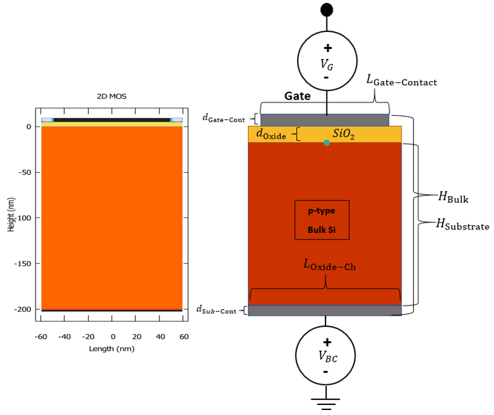
Figure 2.4.15.10 The geometry of the 2D MOS design, and its equivalent geometry from the output file regions.vtr (colored differently in post-processing). The blue circle indicates the position of the origin of our \((x,y)\) coordinate system.
In this tutorial we use a p-doped bulk-Si MOS with a Schottky contact at the gate (instead of a poly-Si contact), and ohmic contact at the substrate. Therefore, the effect of poly-Si depletion at the gate is not present in either of the devices in order to produce the C-V characteristics of our capacitor, which then is the same MOS device used within the N-Ch MOSFET. The bulk p-doping level is \(1 \times 10^{16} \mathrm{cm^{-3}}\), and the oxide layer which consists of SiO:sub:2 has a thickness of \(d_{\mathrm{ox}} = 5 {\mathrm{nm}}\). The length of the channel is \(L_{\mathrm{G}}=100 {\mathrm{nm}}\), the substrate has a height of \(H_{\mathrm{Substrate}} = 200 {\mathrm{nm}}\). The importance of the C-V characteristics of the MOS device derives from the fact, that the charge inversion layer, that is responsible for conduction in the MOSFET, is generated by the capacitive properties of the MOS devices.
Low-Frequency Capacitance
In what follows are the results of our numerical calculations. Concretely, we solve the coupled Schrödinger, Poisson and current equations in two dimensions. We compare our results with the analytic formulas given in standard text books.
The low-frequency capacitance of a MOS capacitor can be measured experimentally with a low frequency signal. In the simple case scenario, the interface trapped charges (charges trapped in the oxide) usually play no role in the capacitance of the device and are not considered in our simulations. Therefore the total capacity of the device is a series connection of the oxide capacitance and the depletion layer capacitance,
The oxide capacitance is the capacitance of the oxide layer, which is independent of the bias, and is simply calculated according to \(C_{\mathrm{ox}} = \varepsilon_{\mathrm{ox}}/d_{\mathrm{ox}}\). This gives a capacitance per unit area (\({\mathrm{F}}/{\mathrm{cm}}^2\)). Multiplying this value with the length \(L_{\mathrm{G}}\) and width \(W\) of the gate gives a capacitance in units of \(\mathrm{F}\).
The depletion layer capacitance is calculated using the charge in the depletion layer as defined in equation (2.4.15.2),
where \(W_{\mathrm{D}}\) is the width of the depletion layer, \(\varepsilon_{\mathrm{s}}\) is the dielectric constant of the semiconductor and \(\varepsilon_{\mathrm{ox}}\) the dielectric constant of the oxide. The depletion layer capacitance is then given by the derivative \(\partial Q_{\mathrm{D}}/\partial \psi_{\mathrm{s}}\), where \(\psi_{\mathrm{s}}\) is the surface potential. Further details on the surface potential can be found in the appendix section. Therefore, the total capacitance calculated according to these formulas would approximately approach the \(C_{\mathrm{ox}}\) at its maximum, would have a flat-band capacitance \(C_{\mathrm{FB}}\) given by the expression in equation (2.4.15.3) , i.e. the capacitance at the voltage, which creates the flat-band condition in the MOS band structure,
with \(L_{\mathrm{D}}\) as the Debye screening length. The Debye length for our MOS capacitor amounts to \(\approx 40.8 {\mathrm{nm}}\), and with that the flat-band capacitance is calculated to be \(C_{\mathrm{FB}} \approx 1.85 {\mathrm{mF/m}^2}\), the equivalent of \(1.85 {\mathrm{pF/cm}}\) if the channel length is \(100 {\mathrm{nm}}\). The C-V curve of the MOS, taking the entire substrate for charge integration, with \(\partial Q_{\mathrm{Sub}} / \partial V_{\mathrm{Bias}}\) is shown in figure Figure 2.4.15.12. Note that the output of the simulations, however, is only the total charge (per cm in 2D), as shown in figure Figure 2.4.15.11, which needs to be (first multiplied with the elementary charge \(|q|\), and then) derived with respect to the bias voltage:
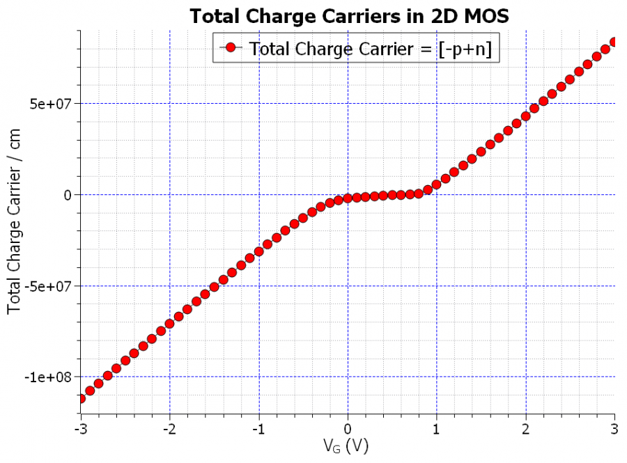
Figure 2.4.15.11 The total charge carriers per cm of the MOS, integrated in the substrate, vs. the applied gate bias.
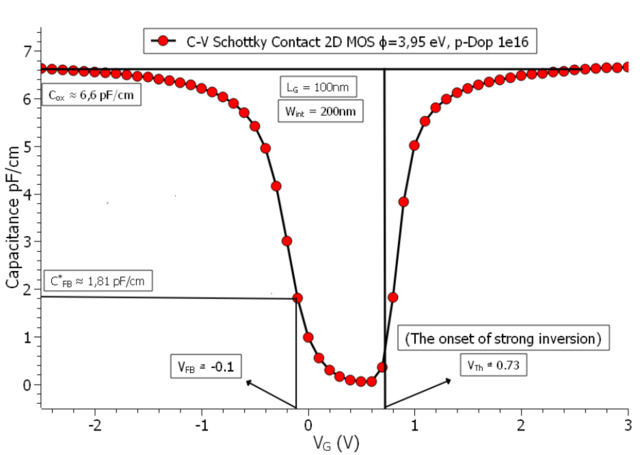
Figure 2.4.15.12 The C-V characteristics of the 2D MOS with \(N_{\mathrm{Sub}}=10^{16} {\mathrm{cm}^{-3}}\) doping concentration in the p-doped silicon substrate, channel length of 100 nm, a Schottky barrier of \(\phi_{\mathrm{B}} = 3.95 {\mathrm{eV}}\), and a charge integration region equal to the entire substrate. (Note that the flat-band voltage has been chosen from the observation of the band edges in the simulation output, which are flat for the bias value of \(-0.1 {\mathrm{V}}\)).
In the above figure the \(C^{*}_{\mathrm{FB}}\) is marked with * because the value measured differs from the calculated value. Later we will show how the C-V curve could be measured, so that the value of the flat-band capacitance is consistent with (2.4.15.3).
There are three values which we read from the graph (actually four but since we have the band edges here in the simulation output, we just need three). The first is the oxide capacitance \(C_{\mathrm{ox}}\), which is approximately the ceiling of the curve. The second is the flat-band capacitance \(C_{\mathrm{FB}}\), corresponding to the value of the flat-band voltage \(V_{\mathrm{FB}}\) (read from the status of the band edges in the simulation output). And the third is the threshold voltage \(V_{\mathrm{Th}}\), which is the onset of the strong inversion. The flat-band condition in the 1-dimensional band edges output is illustrated in figure Figure 2.4.15.13:
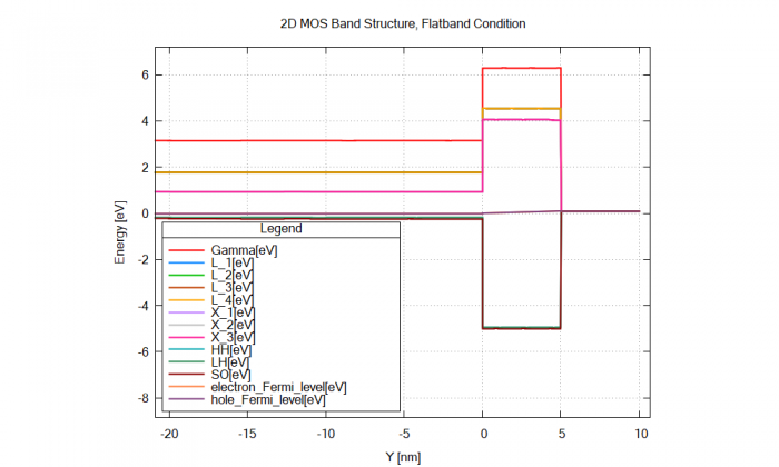
Figure 2.4.15.13 The alignment of conduction and valence band edges with respect to the Fermi levels of the 2D MOS under the flat-band condition along a one-dimensional slice along the y direction. (The lowest conduction band edge is labeled with X.
The bias voltage that results in a band structure in the figure Figure 2.4.15.13, is called the flat-band voltage \(V_{\mathrm{FB}}\). This voltage is related to, and is a part of the definition of the threshold voltage,
The \(\psi_{\mathrm{B}}\) is the distance of the semiconductor Fermi level to the mid-point of the band gap, and it is estimated that the onset of the strong inversion is at the point when the surface potential \(\psi_{\mathrm{s}} \approx 2\psi_{\mathrm{B}}\). This surface potential is estimated to be
Calculating this expression for our system, the surface potential amounts to \(\approx 0.713 {\mathrm{V}}\), while the expression \(\sqrt{4\varepsilon_{\mathrm{Si}}qN_{\mathrm{Sub}}\psi_{\mathrm{B}}}/C_{\mathrm{ox}} \approx 0.073 {\mathrm{V}}\), which is actually the voltage drop across the oxide layer \(V_{\mathrm{ox}}\). Therefore taking the flat-band voltage \(V_{\mathrm{FB}} = -0.1 {\mathrm{V}}\), we arrive at a threshold voltage \(V_{\mathrm{Th}} \approx 0.7 {\mathrm{V}}\), which is somewhat lower than the \(0.73 {\mathrm{V}}\) read from the curve. Indeed the value of the threshold voltage is strongly affected by the value of the Schottky barrier.
The height of the Schottky barrier used here, however, has to reflect the metal-SiO:sub:2 interface barrier, and not the metal-semiconductor barrier. This barrier depends on the metal and its work function that is used, and is therefore different for different metals. It is also mentioned in [Wu], that “the work function of the metal gate has to be properly defined in order to achieve the expected threshold voltage \(\mathbf{V_{\mathrm{Th}}}\)”. Even though that the barrier heights for metals such as aluminum have been reported to be around \(3.15 {\mathrm{eV}}\), the barrier height of metals such as gold (Au), and silver (Ag), have been reported to be around \(4.0 {\mathrm{eV}}\) [Goetzenberger]. Here, in order to arrive at a threshold voltage of \(0.7 \mathrm{V}\), the barrier had to be chosen \(3.95 \mathrm{eV}\).
The Schottky Barrier, Doping Concentration, Depletion Region
In the following part we look at a set of figures, which illustrate various parameter changes, which then lead to variations in the three important values which we want to read from the C-V curve. First would be the threshold voltage, and the flatband voltage, both of which could be influenced by the height of the Schottky barrier, and the doping concentration in the bulk-semiconductor, as figure Figure 2.4.15.14 illustrates:
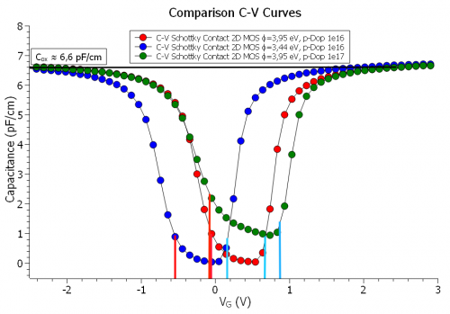
Figure 2.4.15.14 The comparison of the C-V characteristics of the 2D MOS for varying Schottky barrier and the substrate doping concentration, and their effects on the threshold voltage (vertical blue lines), and the flatband voltage (vertical red lines)
As it could be seen in the above figure Figure 2.4.15.14, both the barrier height and the doping concentration shift the threshold voltage \(V_{\mathrm{Th}}\), and the flatband voltage \(V_{\mathrm{FB}}\), however the flatband voltage is more affected by the barrier height rather than the doping concentration. It is also worth mentioning, that the doping concentration alone also affects the minimum capacitance in both low-frequency regime, and the high frequency regime, namely \(C_{\mathrm{min}}\), and \(C^{'}_{\mathrm{min}}\), which are the bottom limits of the C-V curve (\(C^{'}_{\mathrm{min}}\) is directly inversely related to the maximum depletion region width, and apparently so is the \(C_{\mathrm{min}}\)).
In the next set of figures we see, how changing the charge integration region can affect the C-V curve, which then would answer why the \(C^{*}_{\mathrm{FB}}\) in our original curve did not exactly match the calculated flatband capacitance \(C_{\mathrm{FB}}\). The following figure Figure 2.4.15.15, illustrates the effect of changing the charge integration region on the flatband capacitance \(C_{\mathrm{FB}}\):
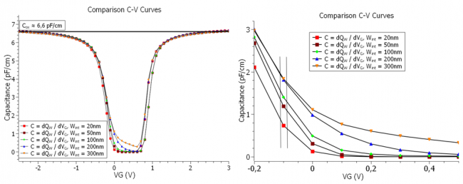
Figure 2.4.15.15 The comparison of the C-V characteristics of the 2D MOS for varying the width of the charge integration region.
And figure Figure 2.4.15.16 shows the C-V curve of the MOS capacitor for a charge integration region of \(W_{\mathrm{int}}=300 {\mathrm{nm}}\):
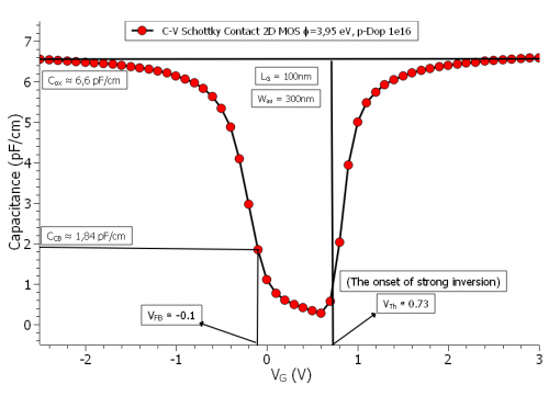
Figure 2.4.15.16 The comparison of the C-V characteristics of the 2D MOS for varying the width of the charge integration region.
Now it seems that the value of the flatband capacitance \(C_{FB}\) in the C-V curve (\(1.84 \mathrm{pF/cm}\)) agrees very well with the calculated value. The reason for that is that, as mentioned in equation (2.4.15.2), the charge in the depletion region is directly proportional to the width of the depletion region. This width has a maximum which is given by:
which turns out to be \(\approx 303 {\mathrm{nm}}\) in our MOS capacitor. Therefore, it should be noted, that in order to be able to reach the flatband capacitance defined by the formalism, the charge integration region should be greater or equal to the maximum depletion region width \(W_{\mathrm{D},max}\). Note that the charge carrier integration has to be specifically mentioned as a region with the following flags in the <nn++_structure{ }_integrate> group:
region{
    rectangle{ # Si Charge Carrier Integration Zone
       x = [-$L_Oxide_Ch/2 , :remove_enter:
       $L_Oxide_Ch/2]
       y = [-$H_Substrate, 0]
    }
    binary{
       name = "Si"
    }
 integrate{
       electron_density{}         # n-charge carriers
       hole_density{}             # p-charge carriers
       label = "Si_Substrate"
     }
 }
The total charge is then \(q(-p_{\mathrm{tot}}+n_{\mathrm{tot}})\). The derivative of this charge with respect to the voltage bias sweep results in the C-V curve, as mentioned before.
Appendix: 2D MOS
The MOS capacitor is a 2D device in its correct form for simulations (with the optional 3rd dimension if need be…). The width of the substrate needs to be somewhat larger than the channel length, so that the depletion layer charges have enough space to expand, also the boundary conditions have to be set to non-periodic in the simulation. That is because even though the channel length is set by the length of the gate-contact, and the inversion layer is bounded by this length, this is not the case for the charges in the depletion layer. Figure Figure 2.4.15.17 illustrates this phenomenon:
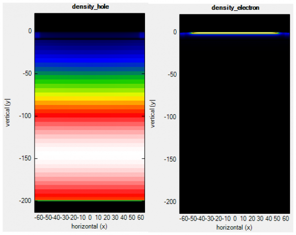
Figure 2.4.15.17 The spatial distribution of charge carriers (electrons) in the inversion layer during inversion, compared to the ones (holes) in the depletion region during depletion.
If we set the substrate width to the length of the channel, which basically would mean that the MOS could also be simulated in 1D, the C-V curve would look like the following in figure Figure 2.4.15.18
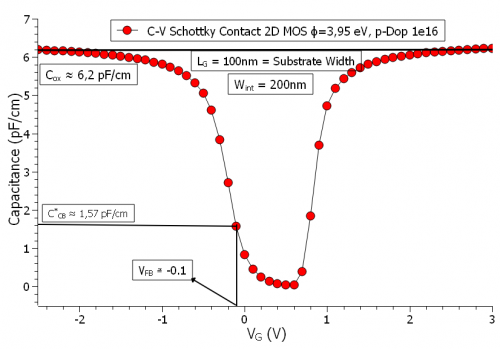
Figure 2.4.15.18 The C-V curve of the quasi 1-D Simulations of the MOS (this is when we set the length of the oxide and the channel-length equal in a 2D simulation and set the boundary condition in x-direction as periodic).
As seen in the C-V curve, not only the oxide capacitance \(C_{\mathrm{ox}}\) is somewhat less than what it should be, the flatband capacitance \(C_{FB}\) (\(1.57 {\mathrm{pF/cm}}\)) does not agree, within an acceptable margin of error, with the calculated value.
With regards to the surface potential \(\psi_{\mathrm{s}}\), it is worth mentioning, that this potential can be measured by measuring the electrostatic potential at the semiconductor-oxide interface, as function of the gate-voltage. For that in nextnano++, one needs to perform a bias sweep at the gate-contact using the template, and make a 1D-section slice of the simulation in the output{ } group, mentioning a range in y-direction around \(y=0\), so that exactly one grid point falls within this range:
output{
  section1D{                 # output a 1D section of the simulation area (1D slice)
    name = "surface_potential"              # name of section enters file name
    x = 0
    range_y = [-0.2, 0.0]    # 1D slice at x = 0 through the middle of the channel
                                            # however limited to the range in y
  }
}
Using the post-processing in the template, one can then construct a curve, which should look like the one shown in figure Figure 2.4.15.19
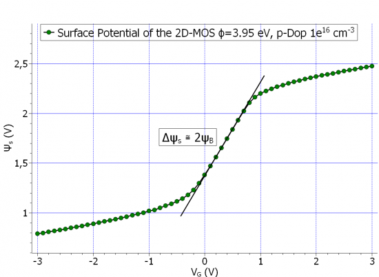
Figure 2.4.15.19 The surface potential, at the semiconductor-oxide interface \(\psi_{\mathrm{s}}\), as a function of the gate.voltage \(V_{\mathrm{G}}\)
Such a curve would go through the origin for an ideal MOS device, however depending on how the electrostatic potential is calculated at the contacts, this curve could go higher or lower on the y-axis. The transition from accumulation to strong inversion of the total capacitance happens basically in the region of the potential, where the line is drawn, for which \(\Delta \psi_{s} \approx 2 \psi_{B}\).
The last remark regarding the capacitance of the MOS could be that, even though the classical formula of parallel plates capacitor is also here applied to the oxide capacitance, in small dimensions and in few nanometer regime, other effects such as tunneling current, and thermionic emissions could play a significant role. Additionally, since the quantum mechanical charge distribution distances itself from the semiconductor-oxide interface (as we shall see in the inversion layer comparison of the MOSFET), these effects would significantly reduce the maximum capacitance of the MOS. As we could see from the C-V curve the flatband capacitance is less than \(30 \%\) of the oxide capacitance, even though one would expect that the \(C_{\mathrm{FB}}\) be somewhere around \(80 \%\) of the \(C_{\mathrm{ox}}\). Therefore if the aforementioned effects be taken under consideration, it could very well be that the \(C_{\mathrm{ox}}\) fall to half of its parallel-plate value.
2D N-Ch MOSFET
Input files:
nMOSFET_2D_Dop-16-20_Schottky_noQM.in
nMOSFET_2D_Dop-16-20_Schottky_QM.in
nMOSFET_2D_Dop-16-20_Schottky_QM_decomposition.in
The MOSFET is a transistor, which is made of a MOS capacitor in the middle and a source-drain channel for conduction. The channel of the MOSFET, which is probably the most important aspect of the MOSFET, extends from source to drain, and is created by a charge carrier inversion layer in the MOS. In this tutorial we simulate an N-channel MOSFET based on the proposed model in [Wu]. As parameters, we vary the oxide thickness, channel length and the doping profiles and investigate how these changes affect the simulation results. These quantities are defined as follows:
\(d_{\mathrm{oxide}}=t_{\mathrm{ox}} = 5 {\mathrm{nm}}\), \(L_{\mathrm{Ch}}=100 {\mathrm{nm}}\), \(N^{+} = 10^{20} {\mathrm{cm}}^{-3}\), \(P= 10^{16} {\mathrm{cm}}^{-3}\).
The overall geometry of the simulated N-Ch MOSFET in this tutorial is illustrated in the following figure Figure 2.4.15.20:
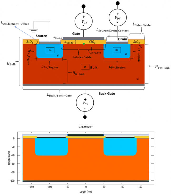
Figure 2.4.15.20 The geometry of the N-Ch MOSFET design, and its corresponding geometry from the output file user_index.vtr. The individual regions can also be found in the output file regions.vtr.
The drain-source current of the MOSFET is given by equation (2.4.15.7)
where the threshold voltage \(V_{\mathrm{Th}}\) is the same threshold voltage for the MOS as defined in equation (2.4.15.4). For the limit of \(V_{\mathrm{DS}} \ll (V_{\mathrm{GS}} - V_{\mathrm{Th}})\) equation (2.4.15.7) reduces to:
For the input characteristics, this equation becomes a function of the gate voltage \(V_{\mathrm{GS}}\) with the drain-source voltage \(V_{\mathrm{DS}}\) kept constant. For the output characteristics, however, this current becomes a function of the drain-source voltage at constant gate voltage. (But rather for a set of gate voltages.) As can be seen the current is directly proportional to the effective mobility \(\mu^{\mathrm{eff}}\), and the oxide capacitance of the MOS capacitor \(C_{\mathrm{ox}}\). Note that \(C_{\mathrm{ox}}\) is the oxide capacitance per unit area in 3D (and per channel length in 2D), and therefore has the units of \(F/(\mathrm{length})^{2}\).
Input Characteristics
Using the Masetti mobility model, we have calculated the input characteristics of the MOSFET classically, which is shown in figure Figure 2.4.15.21 on a linear scale,
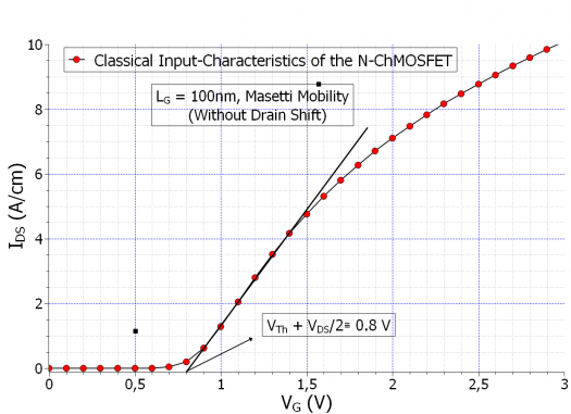
Figure 2.4.15.21 The input characteristics of the N-Ch MOSFET calculated classically with Masetti mobility, showing the position of the threshold voltage \(V_{Th}\).
and in figure Figure 2.4.15.22, on a logarithmic scale:
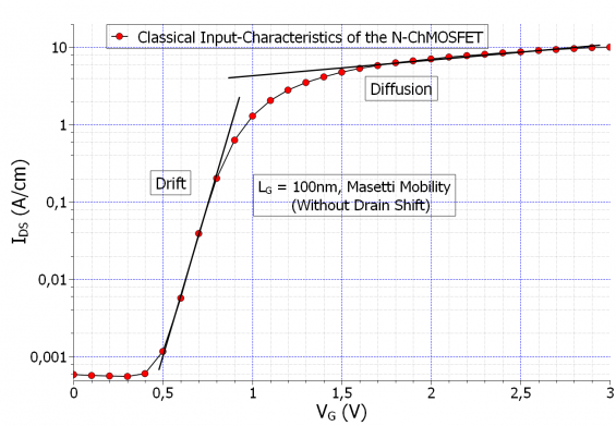
Figure 2.4.15.22 The input characteristics of the N-Ch MOSFET calculated classically with Masetti mobility, showing the drift and diffusion current regions on the logarithmic scale.
The above input characteristics were calculated without the shift in the drain contact. This could modify the results in a certain way that is worth noting. More on this could be found in the Appendix: MOSFET. According to [Sze], the extrapolation of the linear region meets the x-axis at \(V_{\mathrm{Th}} + \frac{V_{\mathrm{D}}}{2}\). Having set the \(V_{\mathrm{DS}}\), to \(0.2 {\mathrm{V}}\), for the calculation of the input characteristics, the value is very well expected to be \(\approx 0.8 {\mathrm{V}}\), since the threshold voltage \(V_{\mathrm{Th}}\) was calculated to be \(\approx 0.7 {\mathrm{V}}\). However we also used a small backgate bias \(V_{\mathrm{BS}}=-0.1 {\mathrm{V}}\) in the above calculations, which slightly modifies the threshold voltage, by changing the voltage drop in the oxide to,
compared to \(V_{\mathrm{ox}} = 0.073 {\mathrm{V}}\). However the difference is negligible in our case. Note that the above input characteristics were calculated without a shift in the drain contact. This can also modify the results to a certain degree as explained in the Appendix: MOSFET section.
However the input characteristics could also be calculated quantum mechanically, since we only have to define the inversion layer region as a quantum region. The prediction is that the charge carrier inversion layer would shift slightly away from the oxide, since the wave function amplitude would have to fall to zero at the oxide-semiconductor interface. This phenomenon is illustrated in figure Figure 2.4.15.23
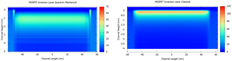
Figure 2.4.15.23 The comparison of the charge inversion layer of the N-Ch MOSFET calculated classically (right), and quantum mechanically (left) at \(V_{\mathrm{GS}} > V_{\mathrm{Th}}\) and \(V_{\mathrm{DS}}=0.2 \mathrm{V}\).
The following set of curves in figure Figure 2.4.15.24 are the comparison of the input characteristics calculated classically and quantum mechanically, with and without quantum decomposition method:
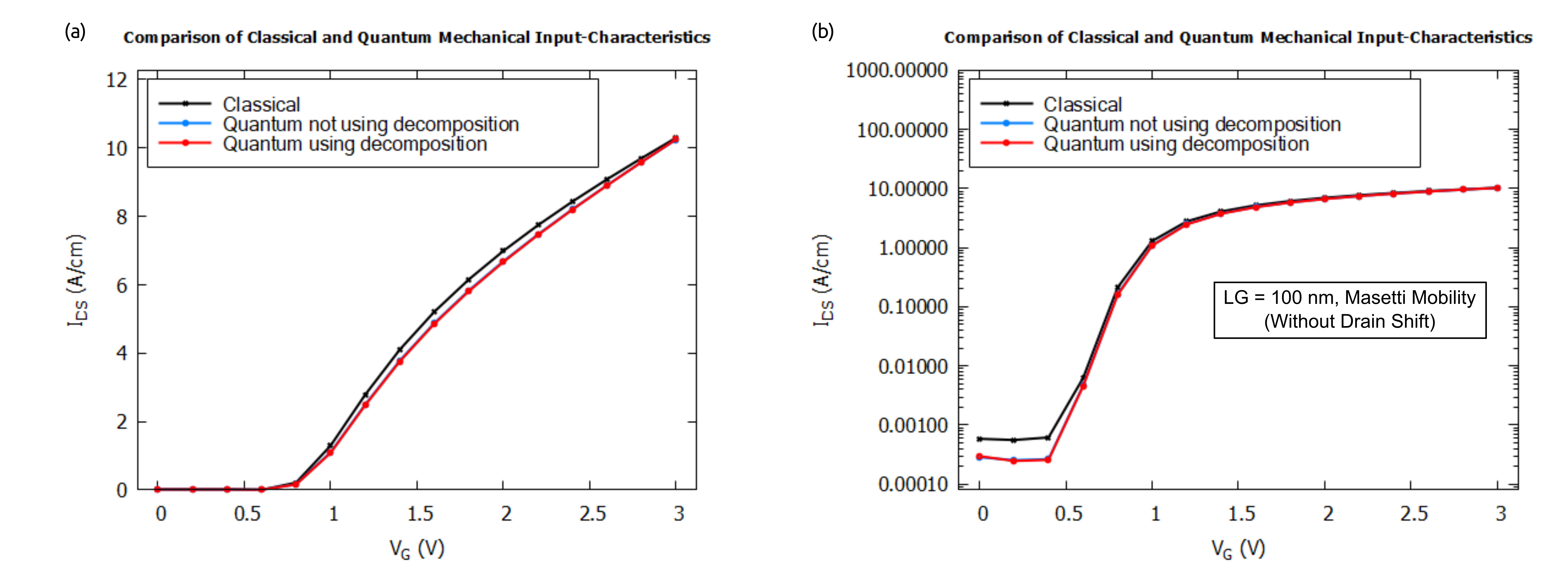
Figure 2.4.15.24 The comparison of the input characteristics of the MOSFET calculated classically and quantum mechanically wit (a) linear and (b) logarithmic scales.
As the simulations shows, there is a slight difference in the input characteristics, most importantly for the leakage current, the one below the threshold voltage. It turns out to be lower for the quantum mechanical input characteristics. Moreover, comparison above shows that using the quantum decomposition method triggered by a keyword quantize_y{} gives almost the same IV curves as in the case of solving the Schrödinger equation in 2D while notably reducing time and memory required for the computation.
Output Characteristics
The output characteristics of the MOSFET is the I-V characteristics of the drain current \(I_{\mathrm{DS}}\) vs. the source drain voltage \(V_{\mathrm{DS}}\), for certain constant gate voltage. Therefore the output characteristics could be viewed as a double sweep, and considering the total simulation time, it is a heavy load on the simulator. With that in mind its worth mentioning that the issue of convergence becomes very important for the output characteristics, in the sense that if the simulation parameters are not chosen correctly the simulations may never converge. More on that could be found in the Appendix: MOSFET. The output characteristics of the MOSFET calculated with the Masetti mobility are shown in figure Figure 2.4.15.25:
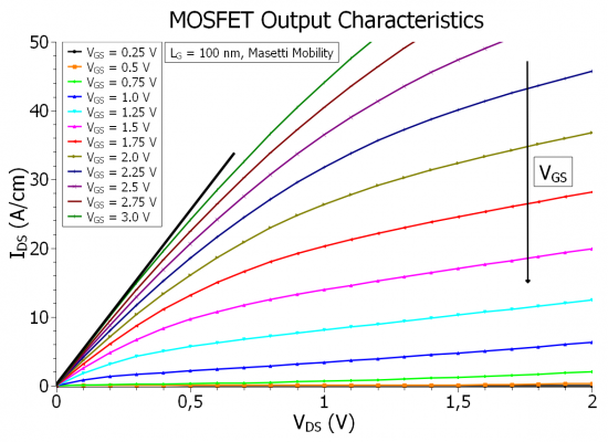
Figure 2.4.15.25 The output characteristics of the N-Ch MOSFET calculated classically with Masetti mobility, showing the linear and the saturation regions of the output characteristics.
The slope of the black line which covers the linear region of all the curves, can be used to calculate the channel specific resistivity. Now, if we take the width of the MOSFET to be \(15 {\mathrm{nm}}\), the output characteristics could be expressed in Amperes, as shown in figure Figure 2.4.15.26:
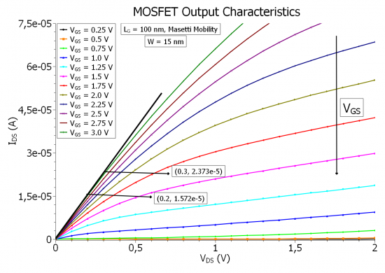
Figure 2.4.15.26 The output characteristics of the N-Ch MOSFET calculated classically with Masetti mobility, showing the linear and the saturation regions of the output characteristics for a width of \(15 {\mathrm{nm}}\).
From the readings on the curve we can estimate the specific channel resistivity,
As mentioned before, the output characteristics can be divided into two regions, the ohmic region and the saturation region. The transition to the saturation region happen at the \(V_{\mathrm{DS,sat}}\), which is give by equation (2.4.15.9):
This value obviously is meaningful for \(V_{\mathrm{GS}} > V_{\mathrm{Th}}\), as it is zero for \(V_{\mathrm{GS}} = V_{\mathrm{Th}}\), and the \(M\) factor is a dimensionless factor equal to \(\approx 1.051\) for our system. The saturation current is then defined as the current that is measured at \(V_{\mathrm{DS,sat}}\), for each \(V_{\mathrm{GS}}\) as defined in equation (2.4.15.10):
and plotting this current over the output characteristics, the curve crosses each \(I_{\mathrm{DS}}\), exactly at the corresponding \(V_{\mathrm{DS,sat}}\) for that output current, as shown in figure Figure 2.4.15.27
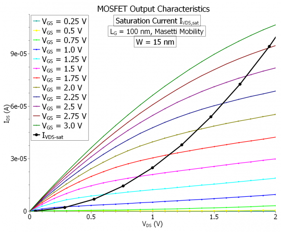
Figure 2.4.15.27 The output characteristics of the N-Ch MOSFET calculated classically with Masetti mobility for a width of \(15 {\mathrm{nm}}\), and the saturation current \(I_{\mathrm{DS,sat}}\) plot.
If we take the effective mobility to be field-independent (which is the case in our simulations), the above \(I_{\mathrm{DS,sat}}\) curve could be fitted with \(I_{\mathrm{DS,sat}} = A \cdot V_{\mathrm{DS,sat}}^2\) formula, where \(A\) is estimated at \(A \approx 2.475 \cdot 10^{-5}\). Note that, the quadratic curve does not meet the output current curves at the points, where they are supposed to meet (at \(V^2_{\mathrm{DS,sat}}\) voltages), because, as we can see, the output charateristic curves do not really saturate after drain source voltage reaches \(V_{\mathrm{DS,sat}}\). This is due to a short channel effect called drain-induced barrier lowering (or punch-through), which we will talk about in last section. When this effect diminishes (as we shall see), the quadratic curve meets the output-curves exactly at the saturation voltage point \(V_{\mathrm{DS,sat}}\).
From the fit parameter estimate, and the rest of the known parameters, we can however estimated the effective mobility \(\mu^{\mathrm{eff}}_{n}\) independent of the field for the short channel case in an approximate way (and compared it later on with the long-channel variant). Taking the oxide capacitance to be \(C_{\mathrm{ox}} \approx 6.6 {\mathrm{mF}}/{\mathrm{m}}^2\), the effective mobility of the electrons is then estimated to be
The calculated bulk mobility from the simulations is given to be \(\approx 933 \mathrm{cm}^2/\mathrm{Vs}\) in the p-doped substrate, and \(\approx 567 \mathrm{cm}^2/\mathrm{Vs}\) at \(y=0\), which is the semiconductor-oxide interface.
Transconductance and Channel Conductance
In many cases, a MOSFET is used for signal amplification, as opposed to switching function, which is the case in CMOS, and digital logic circuits. For this purpose quantities such as transconductance and channel-conductance become important. The transconductance is defined as the derivative of the output current \(I_{\mathrm{DS}}\) with respect to the gate voltage \(V_{\mathrm{GS}}\), for a constant source-drain voltage \(V_{\mathrm{DS}}\):
Figure Figure 2.4.15.28 shows the tranconductance curve and its maximum value:
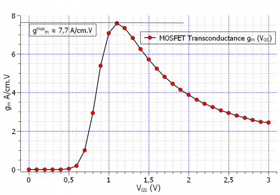
Figure 2.4.15.28 The transconductance of the MOSFET as a a derivative of the source-drain current \(I_{\mathrm{DS}}\) with respect to the gate voltage \(V_{\mathrm{GS}}\).
The maximum value of the transconductance read from the curve amounts to \(\approx 7.7 \mathrm{A/Vcm}\). However, it could also be calculated manually using the equation (2.4.15.11), since we now know the value of the effective mobility:
which amounts to \(\approx 7.9 \mathrm{A/Vcm}\) for an eliminated \(W\) (\(W=1\)). In contrast we have the channel conductance, which is the derivative of the source-drain current \(I_{\mathrm{DS}}\) with respect to the source drain voltage \(V_{\mathrm{DS}}\), at a constant gate voltage \(V_{\mathrm{GS}}\),as defined in equation (2.4.15.12):
which is in turn a function of the gate voltage \(V_{\mathrm{GS}}\). Figure Figure 2.4.15.29 illustrates this conductance for a set of gate voltages:
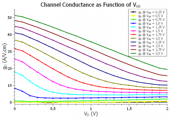
Figure 2.4.15.29 The channel conductance of the MOSFET as a derivative of the source-drain current \(I_{\mathrm{DS}}\) with respect to the source-drain voltage \(V_{\mathrm{DS}}\).
Note that all of the curves in the above figure are from the same family. they are only stretched and displaced with respect to each other since the arguement \((V_{\mathrm{GS}} - V_{\mathrm{Th}})\) acts as a displacement and multiplication factor for the curves for each \(V_{\mathrm{GS}}\).
Finally we have for \(V_{\mathrm{DS}} \geq V_{\mathrm{DS,sat}}\), the saturation transconductance which is derivative of the quadratic current output equation \(I_{\mathrm{DS}}\) in (2.4.15.13) with respect to \(V_{\mathrm{GS}}\):
which would be straight line with respect to \(V_{\mathrm{DS}}\), and \(V_{\mathrm{GS}}\).
Comparison of Different Mobility Models
The effect of the correct mobility model for the simulations of such devices as MOSFETs cannot be overstated. It is an established fact, that the best mobility models used for simulating the current transport in the channel are those that are field dependent, and therefore are modified along the channel as a result of the perpendicular (and also parallel) field. The simplest of these models is the velocity saturation model which sets a maximum value for the drift velocity as the function of the field, and with that the mobility is limited by the maximum velocity. There are of course also more complicated models such as the enhanced Lombardi model, or inversion layer mobility models, which also take into account the scattering of the charge carriers at the semiconductor-oxide interface. These are very specialized models, specifically designed for the simulation of such devices as MOSFETs, and other field effect devices, and are implemented in specialized commercial TCAD tools used by industry. Here we are limited to the already implemented mobility models, which hopefully in the near future will expand. These are the Masetti model, Arora model, Minimos model, and constant mobility model. Figure Figure 2.4.15.30 illustrates the effect of different mobility models on the input characteristics of the MOSFET:
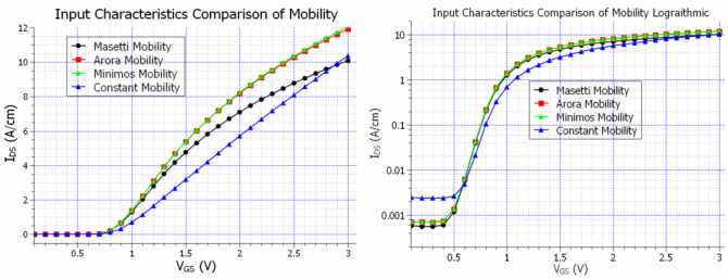
Figure 2.4.15.30 The input characteristics of the MOSFET calculated classically with different mobility models, in normal and logarithmic scales.
In the above curves, interestingly enough the Masetti model seems to reach the saturation much sooner than the other ones, and the constant mobility model seems to be a straight line, even though the value of the constant mobility is much lower in the inversion layer than the rest of the mobility models (\(460 \mathrm{cm^2/Vs}\) compared to \(900-1000 \mathrm{cm^{2}/Vs}\)). The reason for that is that the constant mobility model defines the same electron mobility in the inversion layer, which is a p-doped region, as well as in the source and drain contact regions, which are heavily n-doped regions, whereas the other doping dependent mobility models have significantly different values for these regions, and the fact is that, in order for the current to flow, it must reach the contacts, which are the heavily n-doped regions. That is why the constant mobility produces a different input characteristics curve than the other mobility models. Also regarding the Masetti model, the reason that this model reaches the saturation faster could be attributed to the ratio of the mobility in the p-doped region with respect to the n-doped region, which for the Masetti model is \(\approx 12\), while it is \(\approx 10\) for the Minimos and Arora models. Obviously, this ratio is 1 for the constant mobility model.
The following figure Figure 2.4.15.31 shows the output characteristics calculated with the constant mobility model set at \(\mu_{0} \approx 460 \mathrm{cm^2/Vs}\):
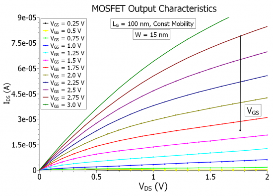
Figure 2.4.15.31 The output characteristics of the MOSFET calculated classically with the constant mobility model, taking the width \(W\) to be \(15 \mathrm{nm}\).
We can now compare this to the Masetti mobility as the example of doping dependent models. Figure Figure 2.4.15.32 shows the comparison for a selection of the \(V_{\mathrm{GS}}\) values:
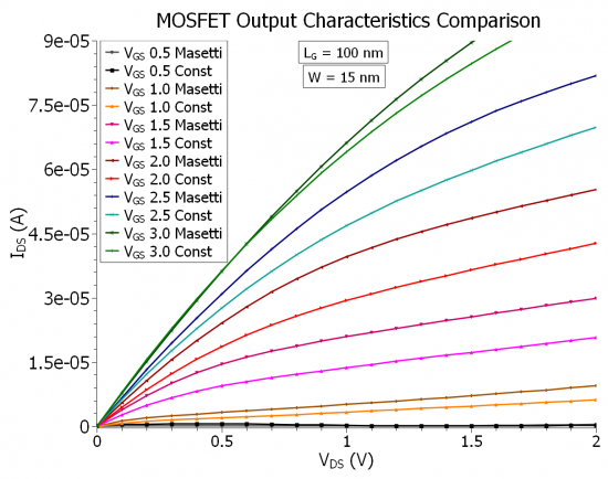
Figure 2.4.15.32 The comparison of the output characteristics of the MOSFET calculated classically with constant mobility and Masetti models, for a selection of gate voltages, and the width \(W = 15 {\mathrm{nm}}\).
As the curves suggest, the difference is negligible for very high and very low gate voltages. The difference becomes significant only for \(1.5 \leq V_{\mathrm{GS}} \leq 2.5 \mathrm{V}\).
Furthermore, it is worth mentioning, that a good mobility model for the inversion layer in the MOSFET should have two field dependencies, one being the perpendicular field originating from the gate, and the other one the parallel field coming from the source-drain bias. The velocity saturation method, which has recently been implemented would only have one of these components, namely the parallel field dependency, and since it is still at the experimental level, we did not put any results simulated with that. However the implementing velocity saturation would have a distinguishable effect on the output characteristics of the short channel MOSFET.
Channel Length Modulation and Pinch-Off effect
nMOSFET_2D_Dop-16-20_Schottky_Class_VG-2.0_Pinch-off.in
One last effect that is worth talking about in the context of the output characteristics, is the pinch-off effect, i.e. the effective shortening of the channel length, which is known as the channel length modulation. It is said that the pinch-off effect steps in at the onset of saturation \(V_{\mathrm{DS}} \approx V_{\mathrm{DS,sat}}\). Figure Figure 2.4.15.33 shows the electron density along the channel for 3 different source-drain voltages (\(V_{\mathrm{DS}} = 0.0 {\mathrm{V}}\), \(V_{\mathrm{DS}} = 0.6 {\mathrm{V}}\), \(V_{\mathrm{DS}} = 1.5 {\mathrm{V}}\)) at a fixed gate voltage \(V_{\mathrm{GS}} = 2.0 {\mathrm{V}}\):
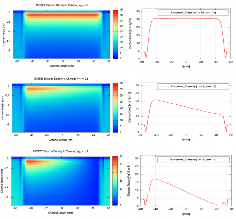
Figure 2.4.15.33 The comparison of the electron density distribution in the channel for \(V_{\mathrm{DS}}=[0.0, 0.6, 1.5] {\mathrm{V}}\) at the gate voltage of \(V_{\mathrm{GS}} = 2.0 {\mathrm{V}}\), showing the pinch-off effect and the effective channel shortening. The 3 pictures of the left show the electron density n(x,y) which is contained in the file density_electron.vtr. The 3 pictures of the right show the content of the file density_electron_1d_middle_line_x_direction.dat which contains a slice along the x direction for constant y value where y lies in the channel for the pictures on the left.
Then the saturation current equation takes the following form:
with \(\lambda \approx \Delta L /L \cdot V_{\mathrm{DS}}\). However this is not an analytical approach, and can possibly lead to inconsistencies. There is a more precise way to calculate the effective channel length, if we take into consideration the depletion widths of the source and drain under potential difference. Figure Figure 2.4.15.34 illustrates these depletion widths:
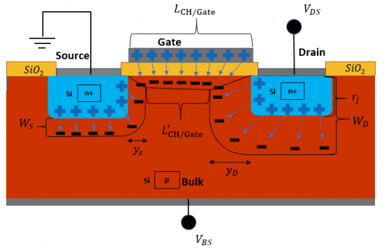
Figure 2.4.15.34 The illustration of the shortening of the effective channel length due to the expansion of the drain and source depletion widths.
Using the built-in potential of the p-n junction at the source and drain \(\psi_{\mathrm{bi}} \approx 0.9 {\mathrm{V}}\), and the surface potential \(\psi_{\mathrm{s}} = 2\psi_{\mathrm{B}} \approx 0.713 {\mathrm{V}}\), we can estimate the length of the effective channel, taking the depletion widths to be approximately equal to \(y_{\mathrm{S}}\) and \(y_{\mathrm{D}}\) for source and drain, within the inversion layer (meaning that the widths also include the surface potential at the semiconductor-oxide interface), as defined in equation (2.4.15.14),
From which then results the effective channel length (as also illustrated in figure Figure 2.4.15.34), as follows:
However, this analysis has an indirect implication with regards to the channel length. Namely, for given source and drain depletion regions there is a minimum channel length. And indeed there is such a consideration, which is said to separate the long channel scenario from the short channel one, meaning a channel above this minimum length is considered a long channel (and not a short channel), and the above considerations apply only to long channel MOSFETs. As we will later see there are also other effects and considerations which will apply to the case of short channels (together known as the short channel effects). The minimum channel length for the long channel case is then given by the following empirical formula in (2.4.15.15),
where \(C\) is a constant, and \(W_{\mathrm{S}}\) and \(W_{\mathrm{D}}\) are the depletion widths of source and drain,
If we take \(V_{\mathrm{D}} = 0.2 {\mathrm{V}}\), then we have \(W_{\mathrm{S}} = 359 {\mathrm{nm}}\), and \(W_{\mathrm{D}} = 393 {\mathrm{nm}}\), while for the same \(V_{\mathrm{D}} = 0.2 {\mathrm{V}}\), the \(y_{\mathrm{S}} = 192 \mathrm{nm}\), \(y_{\mathrm{D}} = 198 \mathrm{nm}\). It makes sense to claim, that a negative effective channel length makes no sense, therefore \(L_{\mathrm{min}} \geq y_{\mathrm{S}} + y_{\mathrm{D}}\). In [Brews] it is mentioned, that the constant \(C\) for device parameters of: \(d_{\mathrm{ox}} = 25 \mathrm{nm}, r_j = 330 \mathrm{nm}, N_{\mathrm{A}} = 10^{14} \mathrm{cm}^{-3}, V_{\mathrm{DS}} = 1 \mathrm{V}, V_{\mathrm{BS}} = 0\), through single point fitting, was measured to be \(0.41 \mathrm{A}^{1/3}\). For this value of the constant, our \(L_{\mathrm{min}}\) would have to be \(198 \mathrm{nm}\), which is almost half the value of \(y_{\mathrm{S}} + y_{\mathrm{D}}\). However, for a value of \(C = 0.8 \mathrm{A}^{1/3}\), we would have a \(L_{\mathrm{min}} = 390 \mathrm{nm}\). Though if we take the fact, that we increase our drain source voltage all the way to \(V_{\mathrm{DS}} = 2.0 \mathrm{V}\), then \(y_{\mathrm{D}}\) would go as high as \(540 \mathrm{nm}\). Then it would be safe to claim, that we need our channel to be at least \(\approx 600 \mathrm{nm}\). Now let us examine the consistency of the \(y_{\mathrm{S}}\), and \(y_{\mathrm{D}}\) values, for a channel length of \(L = 2000 \mathrm{nm}\). The following figure Figure 2.4.15.35 illustrates the pinch-off effect and channel length modulation in the same MOSFET model with a \(L_{\mathrm{G}} = 2 \mathrm{\mu m}\):
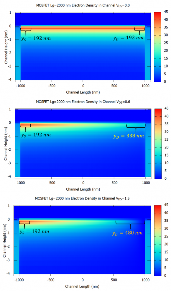
Figure 2.4.15.35 The illustration of the pinch-off effect, and the channel length modulation, in the N-Ch MOSFET with a channel length of \(L_{\mathrm{G}} = 2 \mathrm \mu m\), calculated classically.The depletion widths at the source and drain, \(y_{\mathrm{S}}\) and \(y_{\mathrm{D}}\), estimated from the analytical formulas given above, are indicated.
So therefore, according to the calculations in figure Figure 2.4.15.35, the effective channel length should be \(L_{\mathrm{eff}} \approx 1330 \mathrm{nm}\). Furthermore, it seems that the effects at the boundaries are not compatible with the calculations. However, the shortening of the boundaries due to the applied voltage at the drain is somehow in line with the depletion length \(y_{\mathrm{D}}\).
Short Channel Effects, DIBL and Punch-Through
So as we established in the previous section, our MOSFET, with a \(100 \mathrm{nm}\) channel, length would be below the long channel limit, and therefore would experience short channel effects. The most important of these effects is known as the drain induced barrier lowering (DIBL), which causes the injection of extra charge carriers, resulting in the increasing of the output current even after the saturation \(I_{\mathrm{DS,sat}}(V_{\mathrm{DS,sat}})\). This phenomenon is known as the punch-trough effect and is present in our output characteristics in figures Figure 2.4.15.25 and Figure 2.4.15.26 of the output characteristics section. The DIBL effect is shown in figure Figure 2.4.15.36, comparing two channel lengths:
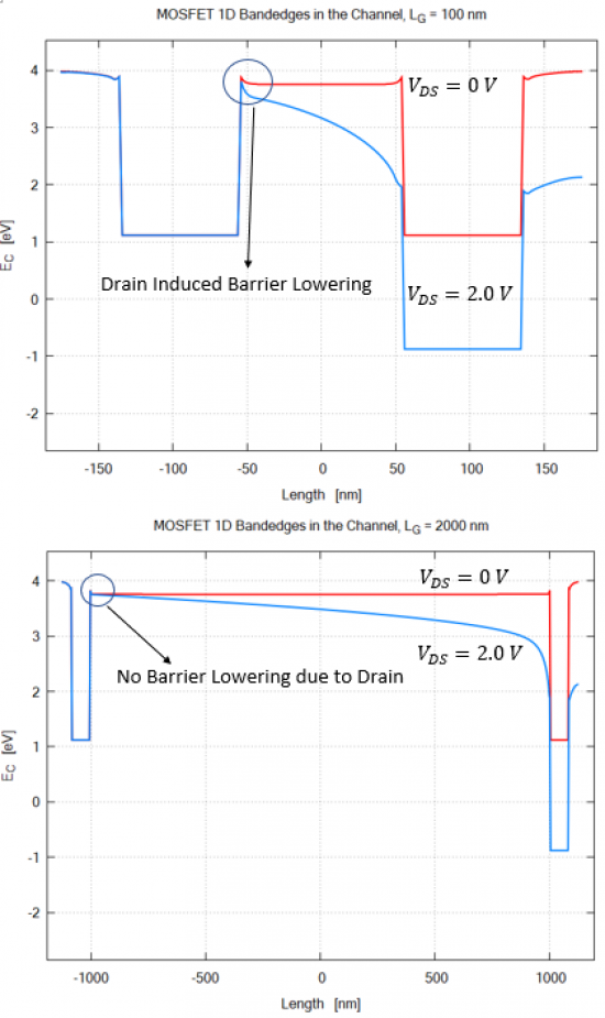
Figure 2.4.15.36 The illustration of the drain induced barrier lowering (DIBL) in \(100 \mathrm{nm}\) gate-length MOSFET, compared to the \(2000 \mathrm{nm}\) gate-length variant (where there are no barrier lowering).
In order to recognize the punch-through effect, the sweep of the gate-length should be performed at high drain-source voltages (for example \(V_{\mathrm{DS}} = 2.0 \mathrm{V}\)) with the input characteristics on a logarithmic scale, which then show if the drift current is limited due to the gate length of the MOSFET. Figure Figure 2.4.15.37 shows this effect:
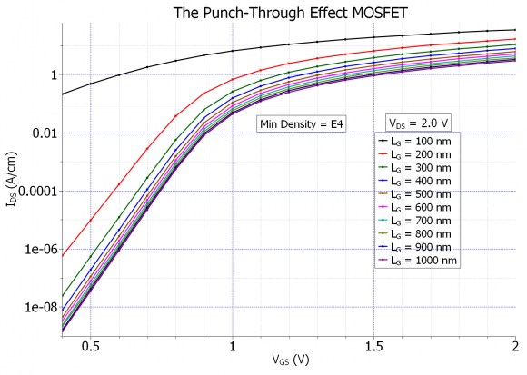
Figure 2.4.15.37 The punch-through effect for a set of channel lengths in MOSFET apparent in the input characteristics (calculated with minimum density of \(\mathrm 10e4\)).
As it could be seen in Figure 2.4.15.37, the MOSFET with gate-length of \(L_G \leq 400 \mathrm{nm}\) would definitely suffer from the punch-through effect. However, one could be safe with a channel length of \(500 \mathrm{nm}\) or \(600 \mathrm{nm}\). Let us now examine the effect of channel length on the normal input characteristics, namely at low drain source voltage. Using the Masetti mobility, the effect of increasing the channel length is illustrated in figure Figure 2.4.15.38:
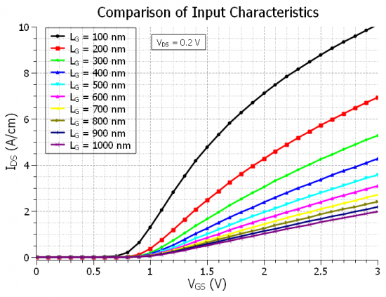
Figure 2.4.15.38 The effect of increasing the channel length on the input characteristics at \(V_{\mathrm{DS}}=0.2 \mathrm{V}\).
So therefore we expect, that our input characteristics will be the same for a channel length of \(400 \mathrm{nm}\) or above using any of the mobilities (Masetti, or constant, or any other), as long as there is no field-dependent saturation in the mobility model. In the following figure Figure 2.4.15.39 let us estimate the threshold voltage for an ideally long channel MOSFET variant (\(L_{\mathrm{G}} = 600 \mathrm{nm}\)):
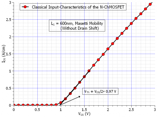
Figure 2.4.15.39 The input characteristics of the long-channel \(L_{\mathrm{G}} = 600 \mathrm{nm}\) MOSFET, calculated with the Masetti mobility, showing the value of the threshold voltage \(V_{\mathrm{Th}}\).
From which it could be concluded, that the threshold voltage is \(V_{\mathrm{Th}} \approx 0.87 \mathrm{V}\). Consequently the output characteristics for the \(L_{\mathrm{G}} = 600 \mathrm{nm}\) MOSFET is shown in figure Figure 2.4.15.40:
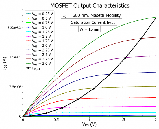
Figure 2.4.15.40 The output characteristics of the long-channel \(L_{\mathrm{G}} = 600 \mathrm{nm}\) MOSFET, showing the diminishing of DIBL effect.
As we can see in the above figure, the quadratic curve fits the output current curves exactly at the proper voltage point, which is \(V_{\mathrm{DS,sat}}\). The fit factor for this MOSFET variant is \(\approx 6.19 \times 10^{-6}\). Using this fitting factor, and taking into consideration the new channel length \(L_{G} = 600 \mathrm{nm}\), we get for the effective mobility:
The calculated mobility from the simulation is once again \(933 \mathrm{cm^2/Vs}\) in the substrate, however it is \(576 \mathrm{cm^2/Vs}\) at \(y=0\) coordinate.
Appendix: MOSFET
In the last section we found out, from the comparison of the input characteristics at high drain-source voltage \(V_{\mathrm{DS}} = 2 \mathrm{V}\), that the MOSFET device with a gate length of smaller than \(L \leq 400 \mathrm{nm}\), would suffer from the punch-through effect. However, if we further shorten our gate length below \(100 \mathrm{nm}\), the situation would even be worse. Namely the leakage current would be so high, that even at very low source-drain voltages \(V_{\mathrm{DS}} = 0.2 \mathrm{V}\), the MOSFET would conduct, even at gate-voltages below the threshold voltage \(V_{\mathrm{GS}} < V_{\mathrm{Th}}\), and therefore the switching capability of the MOSFET would be diminished and eliminated. Figure Figure 2.4.15.41 illustrates this phenomenon:
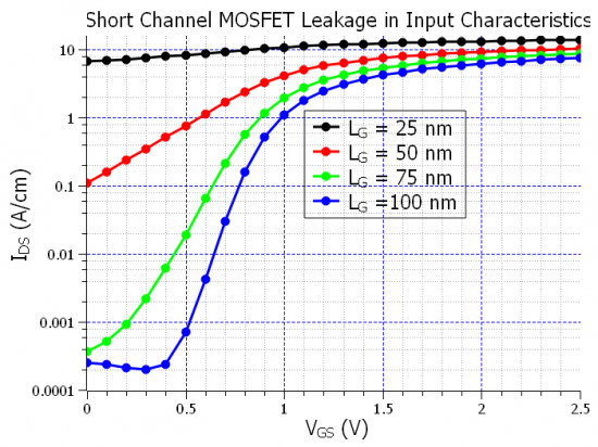
Figure 2.4.15.41 The comparison of input characteristics of the N-Ch MOSFET calculated quantum mechanically with the Masetti mobility, showing the leakage current in the input characteristics.
As the above input characteristics curves show, for gate-length below \(100 \mathrm{nm}\) there is basically no valid switching function possible, as the drift current has already started at \(V_{\mathrm{GS}} = 0 \mathrm{V}\) for \(L_G = 75 \mathrm{nm}\). This is basically to say that, at higher drain-source voltages the leakage curremt is actually more dominant to the channel inversion layer current, which can be switched on and off. It is also worth noting that the leakage current takes place inside the bulk of the MOSFET at the bottom of source drain doped region as figure Figure 2.4.15.42 shows:
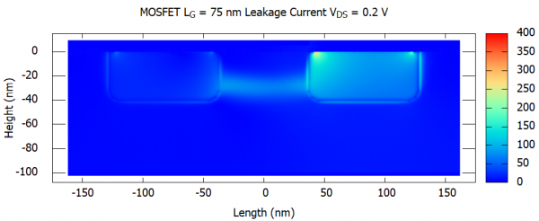
Figure 2.4.15.42 The norm of the leakage current in \(L_G = 75 \mathrm{nm}\) MOSFET, at zero gate-voltage \(V_{GS}=0\), flowing within the bulk.
If we even consider the \(L_G = 25 \mathrm{nm}\) MOSFET, there are certain quantum mechanical affects could be observed. Using the energy_resolved_density{ }, one could observe spacial confinement within the channel at different energy levels. The code has to include the following lines:
classical{
 ...
 ...

   energy_distribution{
       min =  -0.5
       max =  1.0
       energy_resolution = 0.001
       only_quantum_regions = yes
   }

   energy_resolved_density{
       min =  -0.5
       max =  1.0
       energy_resolution = 0.001
       only_quantum_regions = yes
       output_energy_resolved_densities{}
   }

}
But to be able to see the quantum mechanical effects, lets us first take a look at the classical energy resolved densities in the channel and the source-drain doping regions (for that the only_quantum_regions flag has to be set to no in the energy_resolved_density{} group).
The classical energy resolved densities are shown in figure Figure 2.4.15.43:
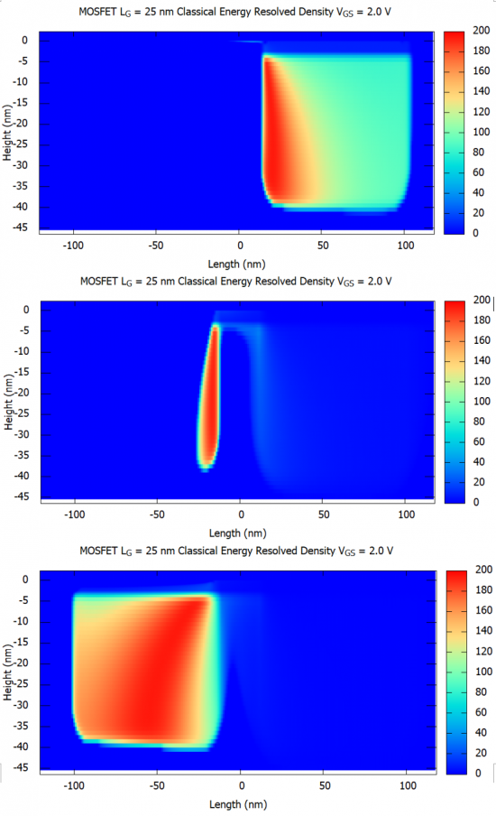
Figure 2.4.15.43 The classical energy resolved density in the \(L_{\mathrm{G}} = 25 \mathrm{nm}\) MOSFET at three different energy levels.
Now let us look at the same energy resolved densities in the MOSFET source and drain region, obtained using the quantum mechanics alone:
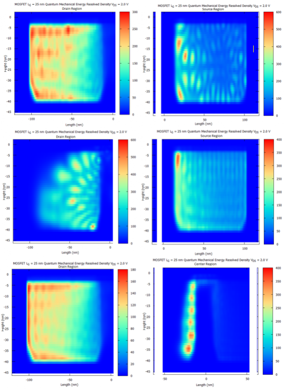
Figure 2.4.15.44 The quantum mechanical energy resolved density in the MOSFET source and drain regions, showing spacial quantum confinement at discrete energy levels.
In the above figure we can clearly see that compared to the classical density, the quantum mechanical density indicate quantum confinement in the source drain doping regions. Furthermore, as we shall see in figure Figure 2.4.15.45, also the density in the inversion layer shows quantum confinement for different discrete energy levels:
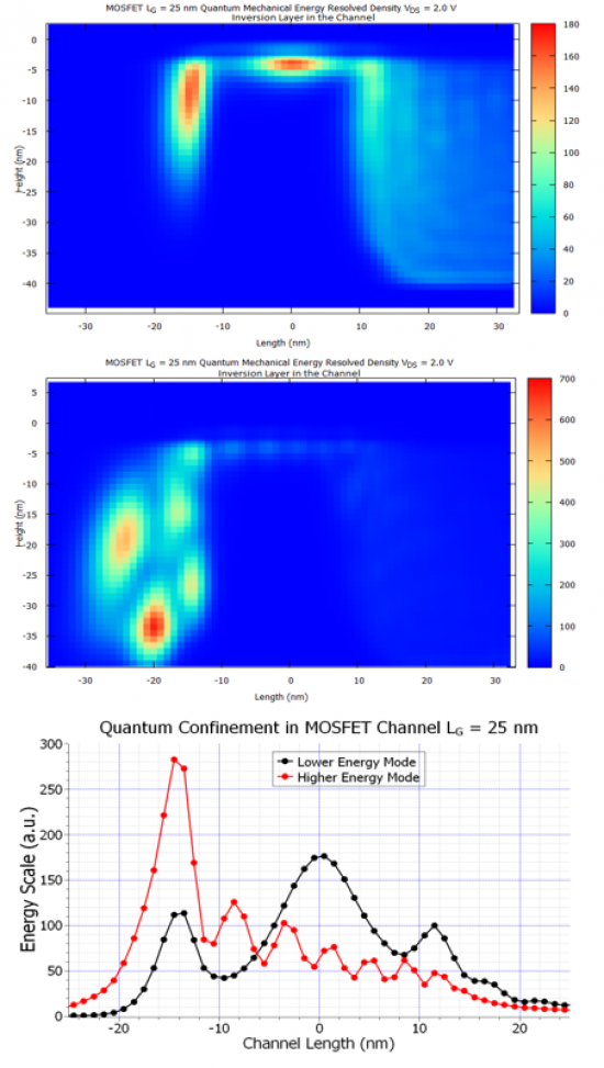
Figure 2.4.15.45 The quantum mechanical energy resolved density in the inversion layer of the MOSFET-channel, at two different energy levels, showing the standing wave pattern, which indicates quantum confinement.
As we can see there is clearly two different quantum confined modes in the inversion layer of the channel for this MOSFET.
With regards to the issue of convergence for the output characteristics, the convergence parameters become very relevant, since for the wrong set of parameters, the simulations may very well never converge and if so might take a significant amount of time.
The key parameter to keep in mind is the ‘’alpha_fermi’’ parameter in current-poisson{ } calculations, which would decide the fate of the calculations.
This parameter needs to be chosen corrently, and also since it will be dynamically reduced, the alpha_scale parameter also need to be set appropriately, with a relatively small alpha_iterations (default is 1000, which is very high!!!), so that a quick adjustment can be achieved if the parameter is too large.
One also needs to significantly increase the number of iterations from the default 100, to a few thousand.
This so called under-relaxation parameter for the quasi-Fermi level is important due to the fact that it decides the volume of the search for the solutions.
Last update: nn/nn/nnnn