From GDSII to Transmission Workflow
Header
- Files for the tutorial located in nextnano++\examples\tricks_and_hacks:
3D_GDS_workflow_template_nnp.in - template for 3D Simulations without gates
3D_GDS_workflow_gdsfile.gds - GDS file
2D_GDS_workflow_transmission_in_2DEG_nnp.in - 2D Simulations
3D_GDS_workflow_script.py - script for importing GDS
- Scope of the tutorial:
Importing layout of gates to a nextnano++ 3D input file
Generating an input file for 3D simulation for a certain bias
Importing a slice of the potential in the 2DEG to a 2D input file
Computing the transmission between two leads.
- Required python packages
gdspy
shapely
- Relevant Keywords (to be updated):
structure{ }quantum{ quantize_x{}}
- Important output Files:
\input files\3D_GDS_input_file_npp.in
\simulations\3D_GDS_Workflow_Results_V_-1.03_npp.in
\outputs\3D_GDS_Workflow_Results_V_-1.03_npp\bias_00000\potential_2d_2DEG.fld
\outputs\2D_GDS_workflow_transmission_in_2DEG_nnp\bias_00000\CBR\transmission_sums_device_Gamma.dat
Within this tutorial we present a convenient methodology of simulating transmission in top-gated structure focusing on the geometrical design of the gates. As transmission of such structures highly depend on the geometry of the gates we propose approach involving usage GDSII files to make the definition of the gates more comfortable. The workflow is presented on the example of the Electron Flying Qubit.
The simulated structure : Electron flying qubit
The implementation of an electron Flying Qubit requires to estimate the changes in the electrostatic potential in the 2DEG region as a function of the applied bias to the QPCs. Depending on the shape of the gates 3D simulations of the gates are required, demanding huge runtime for obtaining the potential at each point of the two-dimensional electron gas formed at a certain depth of the structure. A critical value of the bias that depletes the electrons in this region (the pinch-off voltage) shall be computed with high accuracy. Knowing the pinch-off the transport of electrons in this layer of the structure can be fully controlled.
Nevertheless, the effort for computing the transmission in the 2DEG region can be reduced, if we restrict the simulation to a plane in this region.
This tutorial illustrates this workflow using the structure presented in Figure 2.4.18.16.
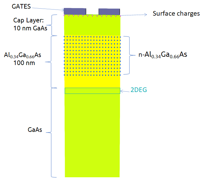
Figure 2.4.18.16 Device under simulation
The two-dimensional electron gas is formed at the interface of the AlGaAs and GaAs (the substrate) materials. Doping the AlGaAs with n-type impurities at a certain distance of this interface improves the confinement of electrons in the 2DEG region. A GaAs layer over the n-AlGaAs region acts as a cap of the device. Finally metallic gates with different geometries are directly deposited on the top of surface. Figure 2.4.18.17 presents several geometries used for testing this methodology.
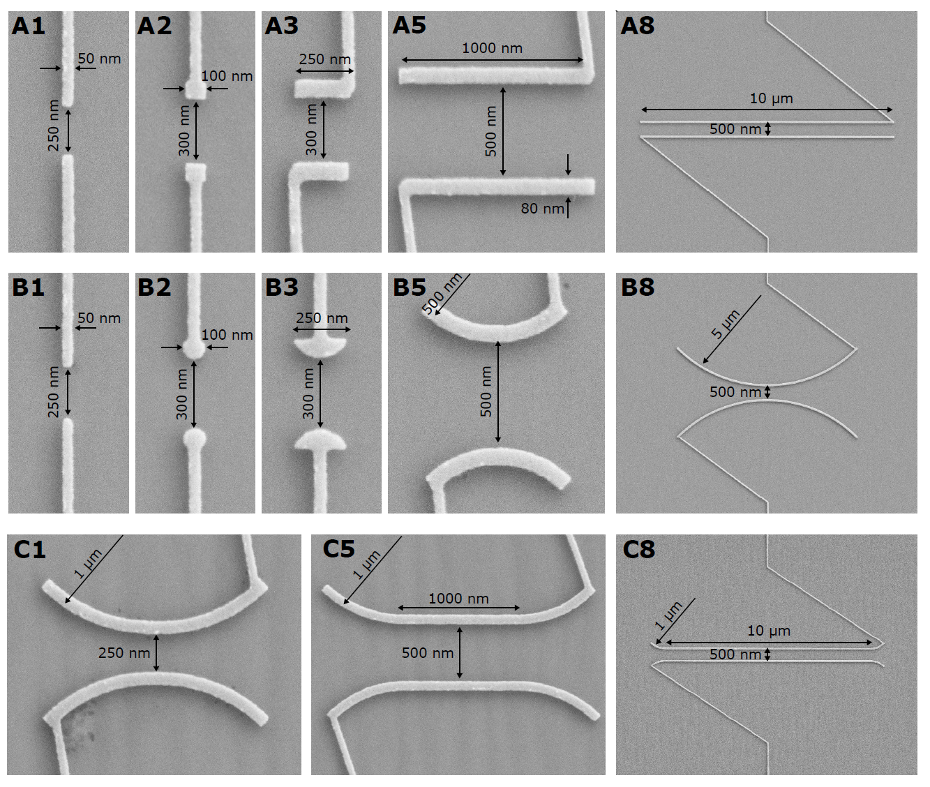
Figure 2.4.18.17 Geometry of the gates used to test this methodology. Source: [Chatzikyriakou_PhysRevResearch_2022]
Work flow
Figure 2.4.18.18 presents a possible methodology for computing the transmission in a channel in the 2DEG plane that provides accurate results and is less workload intensive.
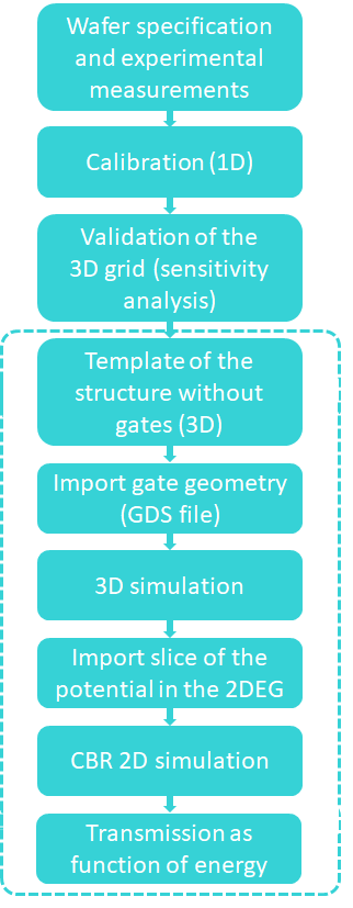
Figure 2.4.18.18 Workflow proposed by this methodology
The main idea is to split the structure in two parts: a stack of layers ( the wafer ) and the parts with more complex geometries.
The wafer specifications and experimental measurements provide the most relevant information for modeling the structure to be simulated. As wafer specifications we mean the different material, alloy composition, doping and thickness of each layer of the device before deposition of the metallic gates on its surface. Experimental measurements, when available, can become a key component for estimation of the surface charges and reduction of the incertainty or the doping concentration of the n-AlGaAs layer.
The combination of these two elements (wafer specification and experimental measurements) provides the required information to calibrate the model. If the experimental measurements are translation invariant on the each layer of the sample, a simple 1D simulation can be used. Nevertherless it is important to validate and to perform a sensitivity analysis of the new grid that will be used in the simulation of the device in three dimensions.
In the case of UltraFastNano we successfully adopted a methodology that provided high accuracy in the estimate of the charge distribution of the manufactured device. This methodology for the calibration was tested for hundreds of geometries of the gates, and it detailed described in [Chatzikyriakou_PhysRevResearch_2022]
As a final result, we can obtain an input file of the calibrated structure without the gates, that we will use as template.
In this tutorial we will not discuss the previous steps in detail, because they are very dependent on the manufacturing and modeling of each specific device under test. The dashed region in the workflow shown in the figure is the one we will discuss in the following sections.
Once we build the template, we can import the geometric information of the gates from a file, for example in GDS format, as we will use as example. We will present a script to perform this operation in a simple way. The resulting input file will be used in 3D simulations, generating automatically the potential in the whole structure, and the corresponding slice in plane in the 2DEG region.
This slice of the electrostatic potential can be exported to a 2D-input file that will compute the transmission between two leads for a certain bias in the gates.
1. Implementing the structure without gates
It is always convenient to start defining an input file that will contains all information of the calibrated wafer with the model that will be used for the whole set of simulations. Our suggestion is to prepare this input file without the region of the QPCs. This will provide more flexibility for simulating gates with different geometries.
In this tutorial our template is the file 3D_GDS_workflow_template_nnp.in that implements the stack of layers of the Figure 2.4.18.16 without the gates.
In nextnano++, the order of the layers in the section structure{ } of the input file it is important.
Each new layer overwrites the previous one. Another important detail it is that the doping is additive, by default.
For this reason, for importing the geometry of the gates to the right position in the new input file, it is necessary to use two identifiers as delimiters of the beginning and the end of the gate region. In our example, we used as identifiers the next labels in the template file:
# --- BEGINNING OF THE GATE REGION --- #
and
# --- END OF THE GATE REGION --- #
as in this snapshot of the template file:
201# --- BEGINNING OF THE GATE REGION --- #
202
203
204# ANY LINE BETWEEN THESE TWO IDENTIFIERS WILL BE REPLACED BY THE
205# GATE SPECIFICATION
206
207# --- END OF THE GATE REGION --- #
It is important that will be exactly two, in order to identify lines in the input file from previous simulations, like calibration, that shall be replaced by the specification of the gates.
2. Importing the geometry of the gates
For this implementation, the GDS file provides 2D polygons that shall be extruded to represent the gates in the 3D representation of the structure. In this particular example, the gates are extended from the coordinates zi = 0 and zf = 17 (nm), where z is the growth direction and z = 0 corresponds to the surface of the device.
From the calibration we can estimate the surface charges and specify them in the input file in terms of a volumetric surface charge concentration, over the whole region of the structure between zis= -1 and zfs= -1 nm.
In the case the gates are defined as schottky contacts, as illustrated in this tutorial, the removal of surface charge concentration just under these gates is necessary.
The script presented above illustrates how to use nextnanopy to import the polygons corresponding to each gate and generates prisms by extrusion of them from the coordinate zi to zf. Additionaly it removes the surface charge concentration only under the gates as mentioned above ( for z in the interval [zis,zfs]). Additional information is added, like the boundary conditions and material adjacent to these gates, when necessary.
For running the script execute python 3D_GDS_workflow_script.py in the command line.
The script assumes that the template file and the GDS files are stored in the folders “templates” and “GDS files” in the same directory where this script is.
Basically it will recognize the identifiers of the gate region in the template and will replace all content between these lines by the imported and processed content from the GDS file as discussed above.
At this point we encourage you to use of nextnanopy for performing the import of the GDS file, although this is not mandatory. Another advantage of using this package is that input files can be automatically modified and executed, and the scripts can be used for documenting each step of your simulation. We remind you that you can find nextnanopy in our GitHub repository at https://github.com/nextnanopy/nextnanopy: it is open source and free!
We prepared a nice Jupyter notebook at docs/examples folder concerning the import of GDS files to a nextnano++ input file.
3. Setup of the input file for 3D simulations
After running the script two different inputs files will be generated:and verify the resulting input file that will be used in the 3D Simulation. It will be stored in the folder input files in the same directory of the script.
\input files\3D_GDS_input_file_npp.in
\simulations\3D_GDS_Workflow_Results_V_-1.03_npp.in
The second is one example for simulating the input file 3D_GDS_Workflow_Results_V_-1.03_npp.in for one specific bias. In this example we will simulate for \(V_{gate} = -1.03\;V\).
In the most general case, 3D simulations can be required for more accurate estimation of the pinch-off voltage. Additionally, in the development of a Electron Flying Qubit building block computation of the conduction band through the whole device is necessary, in order to reproduce the transport phenomena in the 2DEG layer.
As the simulation time depends on the number of the nodes on the grid, for more complex forms and for large devices (of order of microns) with required fine grid ( of order of nm ), some computers shall have not memory enough for the numerical solution of a self-consistent calculation of the Schrödinger and Poisson equations, with a minimum number of wave functions required for such operation.
In this case, a new algorithm was developed within nextnano++ that decomposes the 3D-problem in multiple 1D-problems. In this example, the Schrödinger-Poisson system is solved along the growth direction independently for each pair of coordinates of the nodes of the corresponding perpendicular plane. This decomposition method can be perfect applied to this structure because it is expected that the electrostatic potential does not present any abrupt variation in the any plane perpendicular to the quantization direction. For the application of this algorithm is only required to include the line quantize_x{}, quantize_y{} or quantize_z{} in the quantum{ } section of the input file. In this tutorial the quantum calculations are decomposed in solutions over the growth direction (the z-axis) and, therefore, we use quantize_z{}.
The most important result that will be used in the next steps is the electrostatic potential of the whole structure when a certain bias is applied to both gates. It also generates one slice (a plane) within the 2 DEG region.
For purposes of this tutorial it will be required to simulate the input file \simulations\3D_GDS_Workflow_Results_V_-1.03_npp.in using nextnanomat, for example.
4. Setup of the input file for 2D simulations
The next step in the workflow correspond to the calculation of the transmission of the electrons in a plane in the 2DEG region for a defined bias applied to the gates over the surface (here -1.03V).
We will perform this simulation importing the corresponding slice of the electrostatic potential obtained from the previous section, and will use the Contact Block Reduction (CBR) method, defining two leads in the simulation domain: one at the left border ( lead 0 ) and other at the right border ( lead 1 ). The input file \outputs\2D_GDS_workflow_transmission_in_2DEG_nnp.in is prepared to perform these tasks automatically.
Figure 2.4.18.19 presents the imported slice of the potential. The dashed lines represent the leads of the structure.
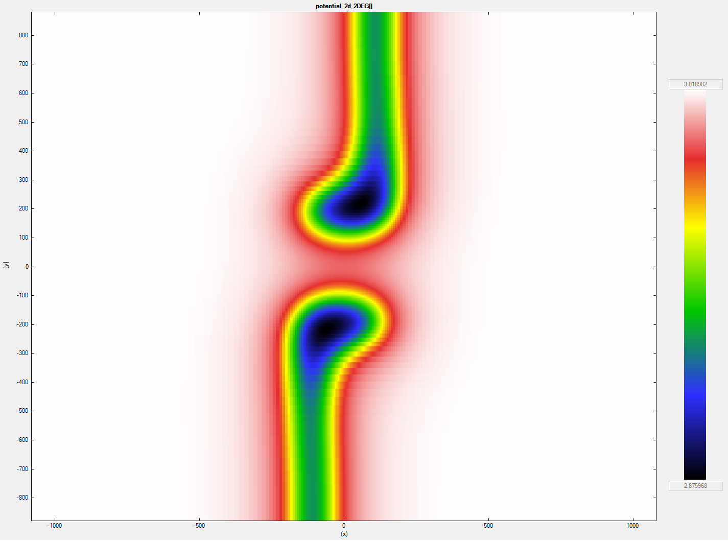
Figure 2.4.18.19 One slice of the potential in the 2DEG region
5. Plotting the transmission through the channel
Figure 2.4.18.19 shows the part of the imported slice of the potential that will actually be simulated when running \outputs\2D_GDS_workflow_transmission_in_2DEG_nnp.in. The image also shows the position of the leads we are considering to computing the transmission. The slice obtained from the 3D simulation at 111 nm under the surface. This results corresponds to the case Vgate = -1.03 V that is still far from the pinch-off voltage for this device, where it is expected several modes can be transmitted through the channel in the 2DEG.
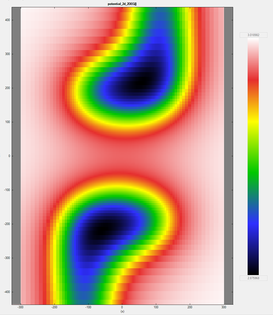
Figure 2.4.18.20 Portion of the slice of the imported potential shown in Figure 2.4.18.19 that will actually be used in the computation of the conductance in the channel in the 2DEG.
As result of the simulation of this input file, we can observe in the folder 2D_GDS_workflow_transmission_in_2DEG_nnp\bias_00000\CBR\transmission_sums_device_Gamma.dat the transmission as function of the energy, shown in Figure 2.4.18.21.
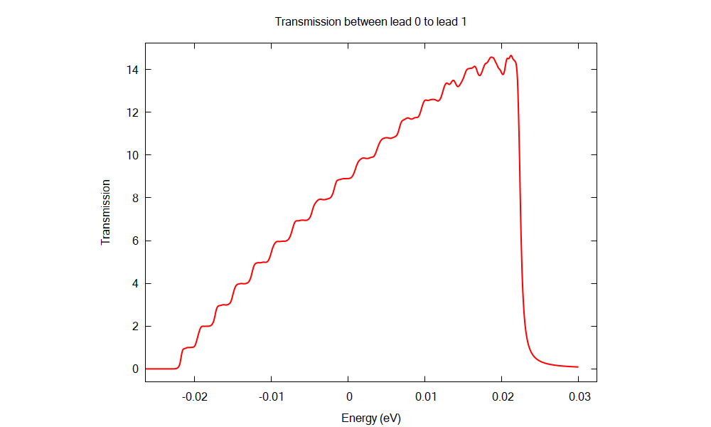
Figure 2.4.18.21 Transmission in the 2DEG region between two leads for \(V_{gate} = -1.03\;V\).
The stepwise behavior of the transmission is consequence of the fact that the conductance is quantized.
- Acknowledgment
This tutorial is based on the nextnano GmbH collaboration in the scope of the UltraFastNano Project aiming at development of the first Flying Electron Qubit at the picosecond scale, and it is funded by the European Union’s Horizon 2020 research and innovation program under grant agreement No 862683.

Last update: 17/07/2024