Surface Charges
- Input Files:
contacts_1D_zero_field_surface_charges_GaAs_nnp.in
contacts_1D_zero_field_surface_acceptors_GaAs_nnp.in
- Scope:
Surface charges on boundaries - comparison to the Schottky barrier
Interface charges (surface states)
Instead of specifying a Schottky barrier, the user can alternatively specify a fixed surface charge density as presented in contacts_1D_zero_field_surface_charges_GaAs_nnp.in. The use of charges is similar as of dopants. One needs to define them for a specific region
structure{
    ...
    region{ # interface charges (surface states)
        line{ x = [10 , 10 + $Width] }
        doping{
        constant{
            name = "negative-interface-charge"   # name of impurity
            conc = $VolumeDensity                # doping concentration [cm-3]
        }
    }
}
and define with some name and given sign.
impurities{
    ...
    charge{
        name = "negative-interface-charge"          # refer to region with name negative-interface-charge
        type = negative
    }
}
Figure 2.5.2.24 shows that the red curve ( = “ohmic” contact with interface charge density \(\sigma\) (surface states) of -8.4796 \(\cdot\) 1012 \(|e|\) /cm2 = -1.3586 \(\cdot\) 10-2 C/m2) is equivalent to the black curve (Schottky barrier of 0.53 eV).
A sheet charge density of -8.4796 \(\cdot\) 1012 cm-2 corresponds to a volume charge of -8.4796 \(\cdot\) 1020 cm-3 if one assumes this charge to be distributed over a grid spacing of 0.1 nm. In this case, the interface charge density corresponds to a Neumann boundary condition for the derivative of the electrostatic potential \(\phi\):
where \(E_x\) is the electric field component along the x direction. \(E_x\) is related to the interface charge as follows:
where \(\epsilon_0\) is the permittivity of vacuum and \(\epsilon_r\) is the dielectric constant of the semiconductor. In this example:
\(\epsilon_r\) = 12.93 for GaAs
\(E_x\) = 1049.7 kV/cm
The output for the electric field (in units of [kV/cm]) can be found in this file: electric_field.dat
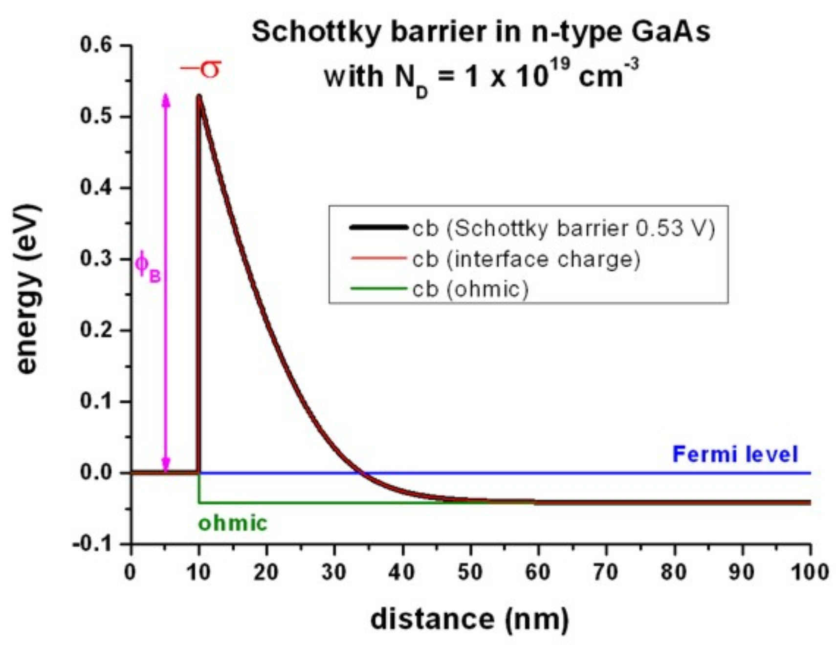
Figure 2.5.2.24 Calculated conduction band profile
The output for the interface densities can be found in this file: material\density_fixed_charge.dat.
Surface states - Acceptors
Input file: 1DSchottky_barrier_GaAs_surface_states_acceptor_nnp.in
Instead of specifying a Schottky barrier, the user can alternatively specify a density of acceptor surface states (p-type doping). Essentially, this can be done by specifying a p-type doping region that is very thin, i.e. the doping is specified only on one grid point.
In this example, we use a doping area of 0.1 nm at the surface that we dope p-type with a volume density of 847.96 \(\cdot\) 1018 cm-3. This corresponds to a sheet charge density of 8.4796 \(\cdot\) 1012 cm-2 where we assume the states to have realistic activation energies.
impurities{
    ...
    acceptor{ # p-type
        name = "impurity_p"
        energy = 0.027 # p-C-in-GaAs (Landolt-Boernstein 1982)
        degeneracy = 4 # degeneracy of energy levels, 2 for n-type, 4 for p-type
    }
}
The results are the same as shown in Figure 2.5.2.24 for the interface charges.
Last update: nn/nn/nnnn