— DEV — n-i-n Si resistor
Attention
This tutorial is under construction
- Input files:
nin-resistor_Si_Sabathil_JCE_2002_1D_nnp.in
- Scope:
This tutorial aims to simulate the current through n-i-n Si transistors. We illustrate our method for calculating the current by studying simple one-dimensional examples that we can compare to full Pauli master equation results. Our method is capable of calculating the electronic structure of a device fully quantum mechanically, yet employing a semi-classical scheme for the evaluation of the current. As we shall see, the results are close to those obtained by the full Pauli master equation provided we limit ourselves to situations not too far from equilibrium. The tutorial is based on the example presented on p. 43 in Stefan Hackenbuchner’s PhD thesis [HackenbuchnerPhD2002] and on the following paper: [Sabathil2002].
- Output files:
bias_xxxxx\density_electron.dat
bias_xxxxx\bandeges.dat
IV_characteristics.dat
Structure
We consider a one-dimensional 300 nm Si-based n-i-n resistor at room temperature where “n-i-n” stands for “n-doped / intrinsic / n-doped” (see Figure 2.4.2.56). The intrinsic region and the n-doped regions are each 100 nm wide. At both ends of the device there are ohmic contacts.
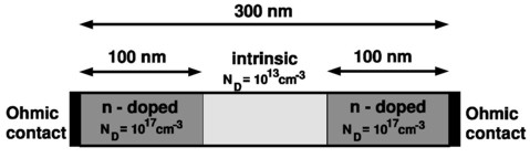
Figure 2.4.2.56 Geometry of the n-i-n Si resistor
The n-doped regions at the left and right sides are doped with a doping concentration of \(N_\mathrm{D} = 1 \cdot 10^{17}\,\mathrm{cm^{-3}}\). The intrinsic region in the center of the device has a background concentration of \(n_\mathrm{i} = 1 \cdot 10^{13}\,\mathrm{cm^{-3}}\) (see p. 43 in [HackenbuchnerPhD2002]). This value is calculated by nextnano++ automatically and does not have to be entered in the input file. Assuming Maxwell-Boltzmann statistics, the intrinsic carrier concentration \(n_\mathrm{i}\) is given by
where \(T = 300\,\mathrm{K}\) is the temperature, \(E_\mathrm{gap} = 1.095\,\mathrm{eV}\) is the band gap energy of Si at \(T = 300\,\mathrm{K}\), \(N_\mathrm{c} = 2.738\cdot 10^{19}\,\mathrm{cm^{-3}}\), \(N_\mathrm{v} = 1.138\cdot 10^{19}\,\mathrm{cm^{-3}}\). Using (2.4.2.1), one obtains \(n_\mathrm{i} = 1.12\cdot 10^{10}\,\mathrm{cm^{-3}}\). For a more detailed discussion of this equation (including Fermi-Dirac statistics), please read the description in Tutorial I-V characteristics of an n-doped Si structure.
The conductivity electron mass is given by
whereas the DOS electron effective mass is given by
The static dielectric constant is given by \(\epsilon = 11.7\). For the donors we assumed an ionization energy of 0.015 eV and a degeneracy factor of 2.
Simulation
The electron density in nextnano++ can be calculated in two different ways:
classical density (Thomas-Fermi approximation)
quantum mechanical density (local quasi-Fermi levels).
The charge density is calculated for a given applied voltage by assuming the carriers to be in local equilibrium that is characterized by energy-band dependent local quasi-Fermi levels \(E_\mathrm{F}(x)\) (i.e. in the simplest case, one for holes and one for electrons). These local quasi-Fermi levels are determined by global current conservation \(\nabla\mathbf{j} = 0\), where the current is assumed to be given by the semi-classical relation \(\mathbf{j} = \mu(x) n(x) \nabla E_\mathrm{F}(x)\), where \(\mu(x)\) is the electron mobility determined by the chosen mobility model. The carrier wave functions and energies are calculated by solving the single-band Schrödinger-Poisson equation self-consistently. The Schrödinger, Poisson and current continuity equations are solved iteratively. As a preparatory step, the built-in potential is calculated for zero applied bias by solving the Schrödinger-Poisson equation self-consistently employing a predictor-corrector approach. The ohmic contacts impose the boundary conditions \(E = 0\,\mathrm{kV/cm}\) on the electric field. For applied bias, the Fermi level and the potential at the contacts are then shifted according to the applied potential which fixes the boundary conditions. The main iteration scheme itself consists of two parts:
In the first part, the wave functions and potential are kept fixed and the quasi-Fermi are calculated self-consistently from the current continuity equation.
In the second part, the quasi-Fermi levels are kept constant, and the density and the potential are calculated self-consistently from the Schrödinger and Poisson equations.
In the input file nin-resistor_Si_Sabathil_JCE_2002_1D_nnp.in the variable $QM at the top of the file can be used for conveniently switching between classical $QM = 0 and quantum mechanical $QM = 1 calculations.
Electron densities
Now let us first have a look at the electron densities at equilibrium (i.e. applied bias \(V = 0\,\mathrm{V}\)) for the cases of classical and quantum mechanical calculations. The electron density is the sum over all three valleys (\(\Gamma\)-point, \(L\)-point and \(X\)-point (or \(\Delta\) for Si) in the Brillouin zone), whereas for Si the dominant valley is the \(X\) valley which is sixfold degenerate (or twelvefold degenerate including spin degeneracy). Thus, we solve Schrödinger’s equation only in the \(X\) valley and take for the other valleys the classical density only. For the quantum mechanical calculation we have to choose appropriate boundary conditions, which are to be specified by the variable $BC_QM at the top of the input file nin-resistor_Si_Sabathil_JCE_2002_1D_nnp.in.
In Figure 2.4.2.57 we compare the classical and the quantum mechanical electron densities for 0 V applied bias. The figure shows quantum mechanical calculating using Dirichlet and von Neumann boundary conditions. Dirichlet boundary conditions force the wave function to be zero at the boundaries and thus the electron density is zero there as well.
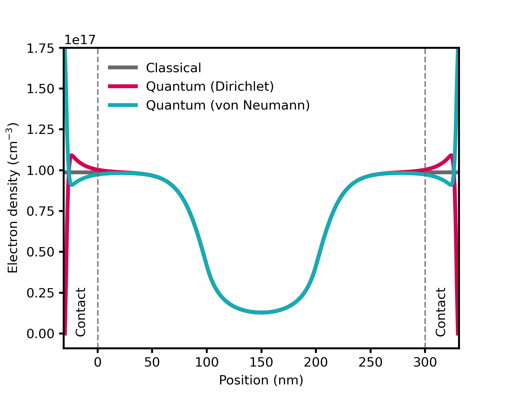
Figure 2.4.2.57 Comparison between classical and quantum mechanical electron densities for the n-i-n resistor. Quantum mechanical simulations using Dirichlet and von Neumann boundary conditions are shown.
I-V characteristics
Now we vary the applied bias from \(0\,\mathrm{V}\) to \(0.25\,\mathrm{V}\) in steps of \(0.05\,\mathrm{V}\) and solve the drift-diffusion equations without taking quantum mechanical densities into account (classical simulation). Here, we compare two different models for calculating the mobility \(\mu\), namely, the constant mobility model (\(\mu = 1417\,\mathrm{cm^2/Vs}\)) and the Hänsch mobility model. The Hänsch model is a high field mobility model, which includes the dependency of \(\mu\) on the electric field.
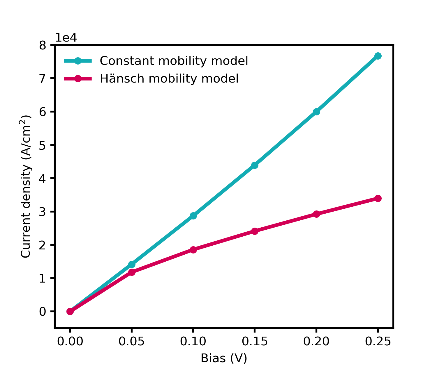
Figure 2.4.2.58 IV characteristics of the 300 nm Si n-i-n resistor for the constant mobility model and high field mobility model Hänsch (classical simulations).
The conduction band edges \(E_\mathrm{c}\) and Fermi levels \(E_\mathrm{F,e}\) (i.e. chemical potentials) for the electrons at different applied voltages are plotted in Figure 2.4.2.59.
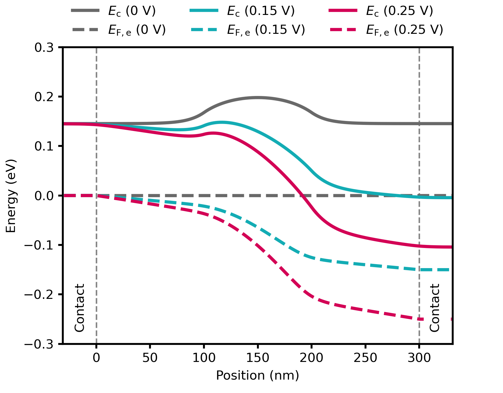
Figure 2.4.2.59 Conduction band edge profile \(E_\mathrm{c}\) and electron quasi-Fermi levels \(E_\mathrm{F,e}\) at bias points of \(0\,\mathrm{V}\), \(0.15\,\mathrm{V}\) and \(0.25\,\mathrm{V}\).
Quantum mechanical calculations
As one may expect, true quantum mechanical effects play little role in this case and both the nextnano++ (i.e. the semi-classical drift-diffusion) and the Pauli master equation approach yield practically identical results for the density and conduction band edge energies (i.e. for the electrostatic potential). We would like to point out that this good agreement is a nontrivial finding, as we calculate the density quantum mechanically with self-consistently computed local quasi-Fermi levels rather than semi-classically.
Figure 2.4.2.60 shows the conduction band edge energies and the electron densities for an applied bias of \(0.25\,\mathrm{V}\). One can see that our results agree very well with the solution of the Pauli master equation [Fischetti1998]. Fischetti obtains for the current density \(6.8\cdot 10^4\,\mathrm{A/cm^2}\), whereas we obtain \(3.65\cdot 10^4\,\mathrm{A/cm^2}\) by using a (semi-)classical drift-diffusion model. However, we note that the current is directly proportional to the mobility in our model, i.e. changing the mobility therefore changes the value of the current. If we had chosen a constant mobility of \(\mu = 1417\,\mathrm{cm^2/Vs}\), then the current at \(0.25\,\mathrm{V}\) applied bias had been \(7.67\cdot 10^4\,\mathrm{A/cm^2}\) (compare with I-V characteristics above).
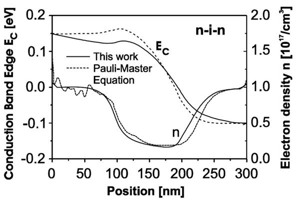
Figure 2.4.2.60 Calculated conduction band edges \(E_\mathrm{c}\) and the electron densities \(n\) of the n-i-n structure as a function of position inside the structure. The results obtained from the Pauli master equation [Fischetti1998] are compared to our quantum mechanical results (full lines).
Conclusion
Here, we demonstrated our approach to calculate the electronic structure in non-equilibrium, where we combine the stationary solutions of the Schrödinger equation with a semi-classical drift-diffusion model. For the electrostatic potential and the charge carrier density, the method leads to a very good agreement with the more rigorous Pauli master equation approach. In addition, the current can also be described accurately.
Last update: nn/nn/nnnn