Optics: Optical gain of InGaAs quantum wells with different strain
- Input Files:
1D_gain_strained_qw.in
- Scope:
Comparison of the optical gain calculated for differently strained InGaAsP-InGaAs quantum wells using 8-band k.p model with [ChuangOpto1995], Sec. 10.4 .
- Most relevant keywords:
quantum{ region{ kp_8band{} } }
optics{ quantum_spectra{} }- Output files:
\bias_00000\Optics\absorption_quantum_region_TEy_eV.dat
\bias_00000\Optics\absorption_quantum_region_TMx_eV.dat
\bias_00000\Quantum\Dispersions\dispersion_quantum_region_kp8_11_00_10.dat
\bias_00000\bandedges.dat
Introduction
We consider a 1D single quantum well system consisting of \(In_{1-x}Ga_xAs\) sandwiched between \(In_{0.71}Ga_{0.29}As_{0.61}P_{0.39}\) barrier layers. Simulations are performed for three different mole fractions \(x\) resulting in three different strain conditions:
\(x = 0.41\) (QW region is compressively strained)
\(x = 0.47\) (QW region is unstrained)
\(x = 0.53\) (QW region is tensely strained).
The parameters for the layer thicknesses, alloy composition and quasi-Fermi levels are taken as follows:
The well widths \(L_\mathrm{w}\) are chosen as 4.5 nm, 6.0 nm, and 11.5 nm for each \(x\) value, respectively, so that the energy difference between the highest valence band eigenstate and lowest conduction band eigenstate would be around 0.8 eV (~1500 nm). The length of the complete simulation region is the same for all three cases, namely \(L_\mathrm{t}\) = 20 nm.
The alloy composition of \(InGaAsP\) barrier region is determined, so that its lattice constant matches to InP substrate and the band gap is 0.95 eV (\(\lambda_\mathrm{g}\) = 1300 nm). The same barrier composition is used for all \(x\).
The electron and hole quasi-Fermi levels were determined for each \(x\), so that the carrier densities of electrons and holes integrated over the QW width both equal 3 \(\cdot\)1012 cm-2.
Computation of the optical absorption spectra within the Fermi’s golden rule and 8-band k.p model is triggered in the optics{} group.
Please refer to our tutorial on absorption for the details about the calculation scheme of the absorption spectra.
Results
We show for each of the three cases the calculated band edges, subband dispersions of the highest electron and hole states, and the optical gain coefficients of TE and TM mode.
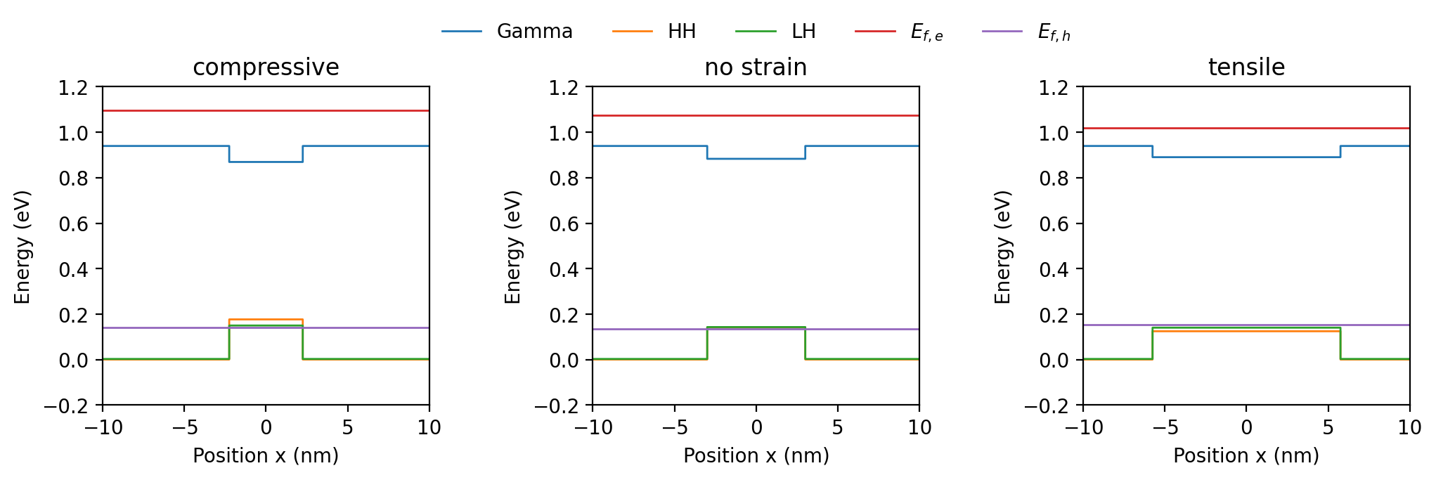
Figure 2.5.12.84 The band edges and Fermi levels of compressively strained QW (\(L_\mathrm{w}\) = 4.5 nm, \(x\) = 0.41) (left), unstrained QW (\(L_\mathrm{w}\) = 6.0 nm, \(x\) = 0.47) (center) and tensely strained QW (\(L_\mathrm{w}\) = 11.5 nm, \(x\) = 0.50) (right). The band profile is shifted so that the valence band edge of the barrier is at 0 eV.
The band profiles for all three cases are depicted in Figure 2.5.12.84. The HH is the highest valence band in the compressive case, HH and LH are degenerated in the unstrained case, and LH is the highest valence band in the tensile case due to the different band-shift of HH and LH. Figure 10.30 in [ChuangOpto1995] shows the same qualitative effect of strain on the band edge profile.
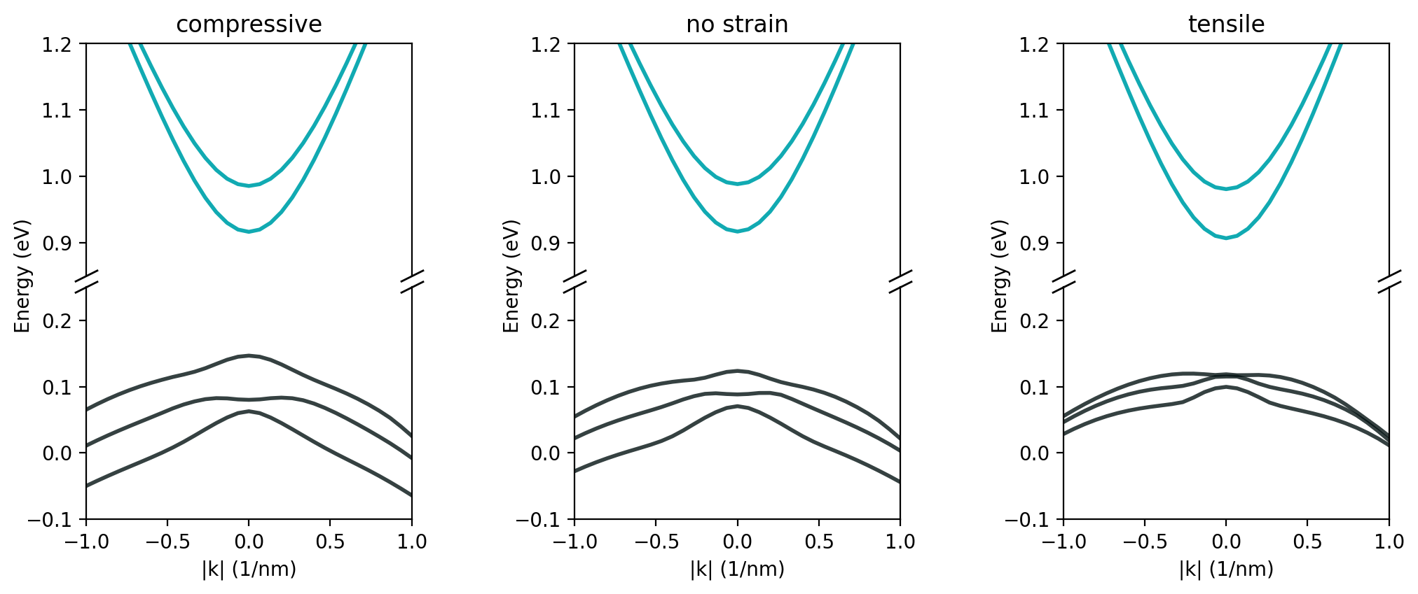
Figure 2.5.12.85 Calculated subband dispersions for the comressively strained QW (left), unstrained QW (center) and tensely strained QW (right). The ground and 1st excited states for electron (cyan), as well as the three highest hole states (black) are shown.
Energy dispersions for all three cases are shown in Figure 2.5.12.85.
The corresponding output file is Quantum/dispersion_~.dat,
which is calculated in quantum{} group. We observe an upward shift of the valance bands going
from compressive to tensile strain, which is in agreement with figure 10.30 in [ChuangOpto1995].
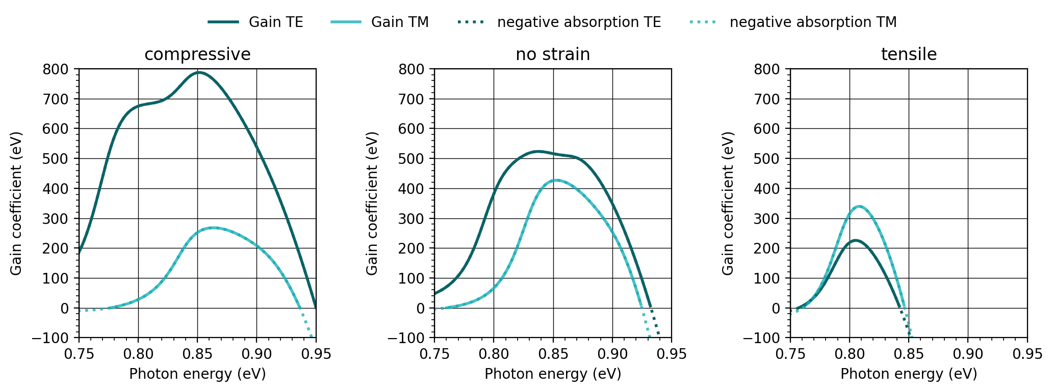
Figure 2.5.12.86 Calculated optical gain of TE and TM optical mode for compressively strained QW (left), unstrained QW (center) and tensily strained QW (right)
Figure 2.5.12.86 shows optical gain computed for the differently strained QWs. The gain for TE polarization is dominant in the compressive and unstrained quantum well as related to transitions involving HH, and TM gain is dominant in the tensely strained quantum well due to the lowest energy transitions involving LH. Comparing the gain spectra with the results presented in [ChuangOpto1995], we observe that for all three cases the shapes of the TE spectra relative to the TM spectra are correctly reproduced. However, there are some deviations in the amplitudes of the spectra. In the cases of the compressive strain and no strain, the computed gain spectra are about 100 cm-2 higher than the ones presented in [ChuangOpto1995]. Conversely, the spectra computed for the tensely strained quantum well are about 100 cm-2 smaller than those in the reference.
Discussion
Most possible reasons which account for the deviations between our gain spectra and these shown in [ChuangOpto1995] may be differences in:
the model applied to compute the spectra,
the number of electron and hole states included in the model,
how the surface charge concentration of 3 \(\cdot\)1012 cm-2 is calculated. In [ChuangOpto1995] the surface charge concentration is equal to \(nL_\mathrm{z}\), where we assumed an integration of the carrier density over the well width, i.e. \(\int n(x)dx\). The surface charge concentration is an important parameter, because it determines the quasi-Fermi levels and therefore the amplitude of the gain spectrum.
boundary conditions for the wave functions. Here, we used periodic boundary conditions.
Last update: nn/nn/nnnn