Optics: Optical gain and spontaneous emission rate of strained GaN quantum well
Section author: Naoki Mitsui
Warning
This tutorial is under construction
In this tutorial, we calculate the optical gain and spontaneous emission rate of strained GaN quantum well using 8-band k.p model implemented in our optics{ } section. This tutorial aims to reproduce the results obtained in [ChuangIEEE1996]:
Related files
Chuang_1996_IEEE_GaN_QW_nnp.in
Chuang_1996_IEEE_GaN_QW_postprocess.py (python script using nextnanopy)
Table of contents
nextnano++ can calculate the spontaneous emission rate and optical gain in 2 different models.
“Semiclassical” calculation corresponds to classical{}
“Quantum” calculation corresponds to optics{ }
For the 1st model, please refer to InGaAs Multi-quantum well laser diode. Roughly speaking, this model calculates the carrier densities either quantum mechanically or classically and the emission rate is calculated from them in a phenomenological way (2.5.4.4).
The calculation described here is the 2nd model. This starts from the Fermi’s golden rule (time-dependent perturbation theory) and electrons in a condensed matter are treated fully quantum mechanically. This model has the following characteristics:
able to take into account the band-bending and band-mixing effect by strain
distinguishes the different polarization
requires less phenomenological parameter
require the k.p parameters instead
(For most of the important materials, the parameters are already included in our database file.)
Structure
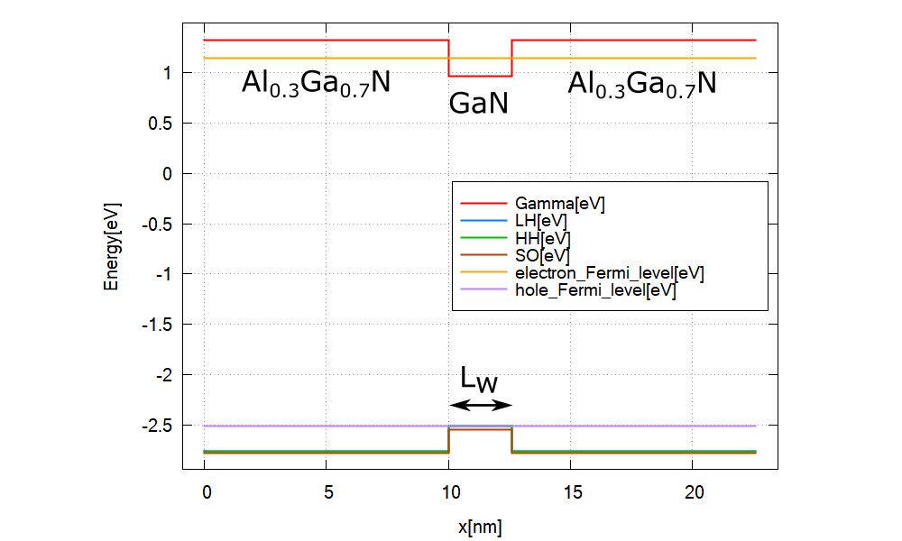
Figure 2.5.12.87 The band edges and Fermi energies for Al0.3Ga0.7N-GaN quantum well with the carrier concentration \(n=3\times 10^{19}\) cm\(^{-3}\) inside the well region.
The above figures show the Gamma band edge of the Al0.3Ga0.7N-GaN quantum well.
Please see the input file for the details.
The parameters used in this simulation are as follows.
Property |
Symbol |
Value [unit] |
|---|---|---|
quantum well width |
\(L_w\) |
2.6, 5.0 [nm] |
doping concentation |
\(N_D\) |
0 [cm-3] |
carrier concentration in the well |
\(n\) |
1, 2, 3 \(\times\) 1019 [cm-3] |
linewidth (FWHM) |
\(\Gamma\) |
0.0132 [eV] |
temperature |
\(T\) |
300 [K] |
Note
The piezo- and pyroelectricity are not yet taken into consideration here for the simplicity.
Results
Spontaneous emission rate
The formula used for the spontaneous emission calculation in optics section is as follows:
For the detail of the definition of each quantity and calculation scheme, please see our Optical absorption for interband and intersubband transitions.
Here we show this \(r^{spon}(\vec{\epsilon}, \omega)\) calculated for \(L_w=2.6\) [nm], \(L_w=5.0\) [nm] and each polarization. These results well agree with Fig.7 of [ChuangIEEE1996].
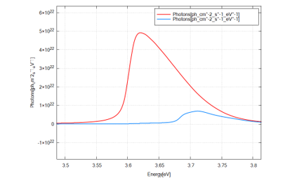
Figure 2.5.12.88 \(r^{spon}\) for an Al0.3Ga0.7N-GaN quantum well with the carrier concentration \(n=3\times 10^{19}\) cm\(^{-3}\) on each polarization TE (x or y) and TM (z). \(L_w=2.6\) [nm]
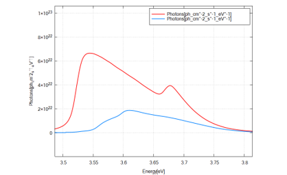
Figure 2.5.12.89 \(r^{spon}\) for an Al0.3Ga0.7N-GaN quantum well with the carrier concentration \(n=3\times 10^{19}\) cm\(^{-3}\) on each polarization TE (x or y) and TM (z). \(L_w=5.0\) [nm]
When we don’t apply the linewidth broadening, the result shows the exact energy where the emission by each pair of state starts.
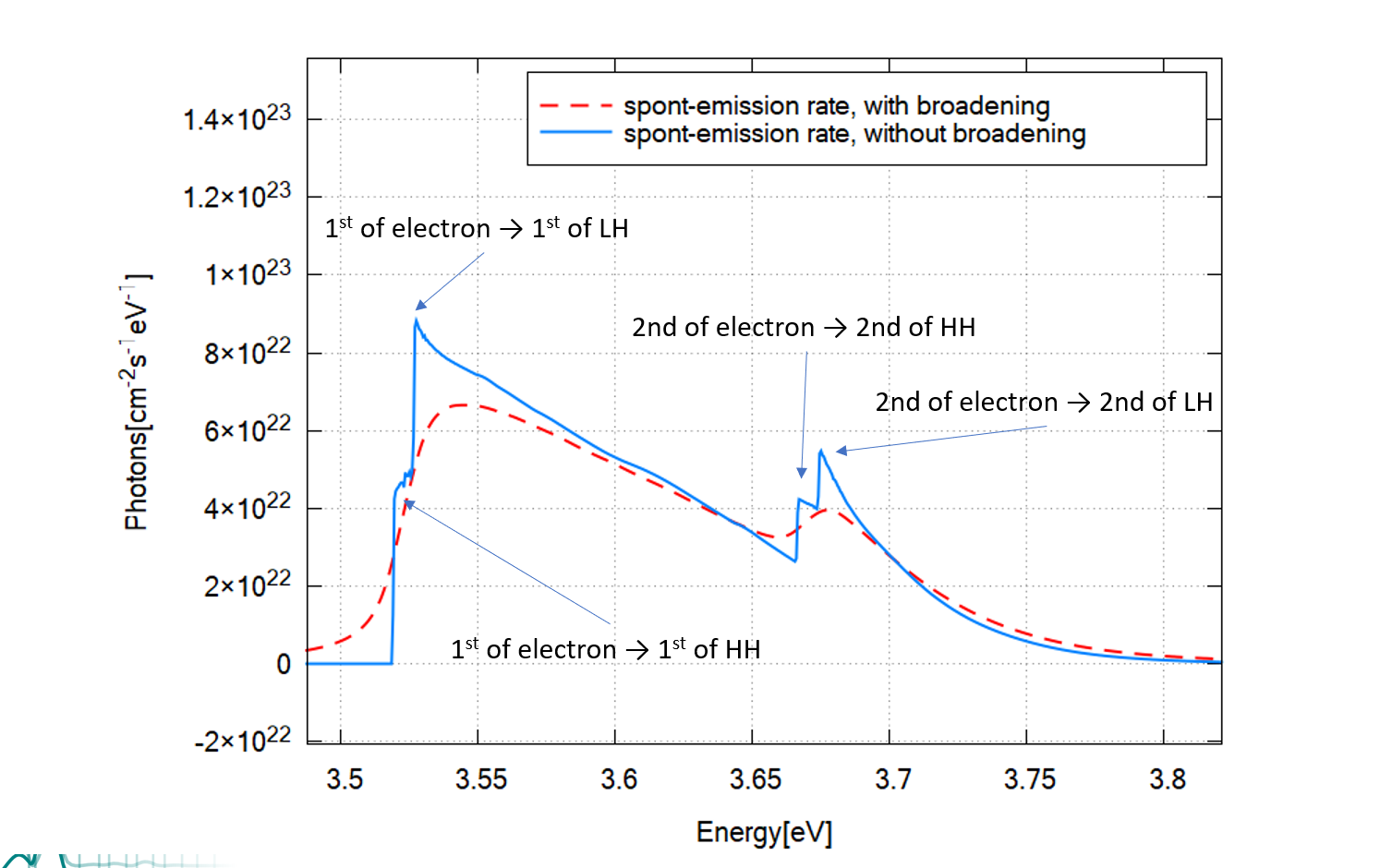
Figure 2.5.12.90 TE emission rate in Figure 2.5.12.89 with (red dashed line) and without (blue line) line width broadening.
Optical Gain
The optics section can calculate the absorption spectra \(\alpha(\vec{\epsilon},\omega)\). This can be understood as a negative gain, i.e.
For the details of the calculation scheme of \(\alpha(\vec{\epsilon},\omega)\), please see our Optical absorption for interband and intersubband transitions.
Here we show this \(g(\vec{\epsilon}, \omega)\) calculated for \(L_w=2.6\) [nm], \(L_w=5.0\) [nm] and polarization.
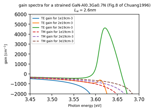
Figure 2.5.12.91 \(g(\vec{\epsilon},\omega)\) for a Al0.3Ga0.7N-GaN quantum well with the carrier concentration \(n=1,2,3\times 10^{19}\) cm\(^{-3}\) on each polarization TE (x or y) and TM (z). \(L_w=2.6\) [nm]
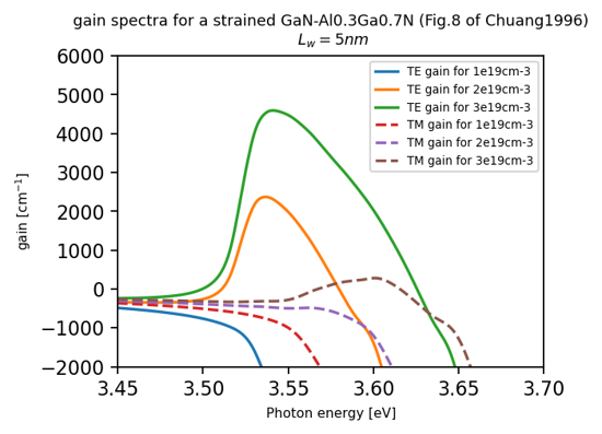
Figure 2.5.12.92 \(g(\vec{\epsilon},\omega)\) for a Al0.3Ga0.7N-GaN quantum well with the carrier concentration \(n=1,2,3\times 10^{19}\) cm\(^{-3}\) on each polarization TE (x or y) and TM (z). \(L_w=5.0\) [nm]
These results almost agrees with Fig.8 of [ChuangIEEE1996] except for the case when the gain peak is relatively low. This is because the models used here and [ChuangIEEE1996] apply the linewidth broadening in different steps.
Last update: nn/nn/nnnn