Reducing dimensionality of 3D input files
- Input Files:
Large_device_simulation_1D_version_nnp.in
Large_device_simulation_2D_version_nnp.in
Large_device_simulation_3D_version_nnp.in
- Scope of the tutorial:
Guidelines for reducing dimensionality of 3D-input files
Refining the grid line spacing efficiently
Impact of the grid resolution and the number of nodes in the grid on the simulation time
- Introduced Keywords:
global{ simulate1D }
global{ simulate2D }
global{ simulate3D }
grid{ xgrid{ } ygrid{ } zgrid{ } }
quantum{ region{boundary_conditions{}} }
strain{ growth direction }}
structure{ line{} }
structure{ rectangle{} }
structure{ cuboid{} }- Relevant output Files:
\bias_00000\bandedges.dat
\bias_00000\bandedges_1d_xz_Si_2DEG.dat
Large_device_simulation_2D_version_nnp.log
Accurate simulations depend on finding a compromise between a very fine grid, the memory consumption and the corresponding runtime. Nevertheless tuning the grid resolution for 3D simulations of large devices can become highly time expensive, when a methodological approach is missing.
The purpose of this tutorial is to provide some suggestions with the aim of reducing the time for choosing a suitable grid and of its impact on the solutions. It is part of the methodology Approaching big 3D designs with Schrödinger-Poisson self-consistent solver, that we strongly recommend being followed.
In this first step we will show what we can learn from simulations in 1D and 2D of the device, for building a suitable grid when modeling the most important regions on it.
To make it very practical, we will introduce in the next section a structure that can be used in a semiconductor-based quantum computer as an example. The quantum operations are performed by handling the bias of gates on the top of the device, that controls the transport of the carriers through the active region. This is a typical device where all transport of carriers is electrostatically dominated. For this reason, a consistent simulation of the charge distribution and the potential in the device is imperative to reach accuracy enough to identify the most important modes of operation at each position.
Most of these devices can present hundreds of nanometers than represent a heavily time-consuming procedure when performing 3D simulations. The suggestions presented below will assist you to define the grid that can reduce the bottlenecks of larger simulations. There is not a unique way to do it, but it has been used for numerous cases, not only for quantum computing, and provided very good results in most of them.
Device to be simulated
Figure 2.5.17.6 presents a simplified version of a device that consists basically of a 7 nm-Si layer buried in a silicon dioxide structure [Kriekouki2022]. This silicon layer will be used as the channel where electrons can transit through.
Gates ( FGS, FGD, LG1, LG2, LG3 ) are deposited at few nanometers of top of the interface of the Si channel with the surrounding oxide gates. By applying specific combinations of biases to these gates it is possible to change the electrostatic potential and, in this way, to control the states present in the structure for each configuration. The source and drain contacts can be seen as the reservoirs that will provide the carriers that will propagate in the channel.
Additionally, applying bias to a back gate under the thick layer of oxide under the Si-channel can allow or prevent the transport through the device.
The dimensions of this device to be simulated is the order of 400 nm x 800 nm x 70 nm. The last dimension ( 70 nm ) does not include the back gate and substrate regions that, as we will see soon, can be removed from the simulation domain. Nevertheless, the relevant results in the active regions are very localized and can require grid resolutions of order of few nanometers or smaller.

Figure 2.5.17.6 Device to be simulated. The Si-channel is buried in the oxide. FGS, FGD, LG1, LG2, and LG3 are used to shape the electrostatic potential.The back gate is used to allow or to interrupt the transport of electrons through the channel. The source and drain are the reservoirs of carriers.
Reducing the dimensionality of the problem
Before setting up input files for 3D simulations we recommend to start with 1D or 2D computations. Even when quantum computations are necessary, use only semiclassical models ( Poisson ), just enough to identify the most relevant aspects of the transport in some critical regions.
You can either start designing the 3D version and reduce it to the 1D and 2D versions, or to develop first the 1D version and expand it to the final 3D structure.
For making the design more flexible, use variables to represent the most important coordinates of the structure.
Name the variables according its 3D representation in the device reference frame, in contrast to the simulation reference frame.
The simulation system is defined in the global{} section of the input file.
Figure 2.5.17.7 presents the most important coordinates in the device coordinate system, used in all versions of the input files of our example.

Figure 2.5.17.7 Device reference system and most important coordinates used for 1D and 2D simulations: (a) the 3D representation, (b) structure definition, and (c) structure after applying boundary conditions to the contacts and gates. Dotted lines ( in red ) represent sections defined in the input files.
Here is an example how to perform the modification from 3D to 2D input file. Suppose that one region is defined in the 3D input file by:
cuboid{
     x = [$x_3F, $x_3L]
     y = [$y_4GS, $y_4GD]
     z = [$z_EG, $z_2F]   # growth direction in the simulation reference system for 3D simulations
}
where the growth direction is along the z-axis ( vertical ) in the device coordinate system.
This has to be translated to a 2D-input file as:
rectangle{
     x = [$y_4GS, $y_4GD]
     y = [$z_EG, $z_2F]   # growth direction in the simulation reference system for 2D simulations
}
and to a 1D-input file as:
line{
     x = [$z_EG, $z_2F]   # growth direction in the simulation reference system for 1D simulations
}
Avoid renaming variables when changing from one dimension to another.
Why this is important?
In nextnano++ the growth direction is aligned to different axis, depending on the dimensionality of the simulation. For 1D simulations, the x-axis of the simulation system is the growth direction. Nevertheless, when we change to the 2D version, the code interprets that the y-axis as the growth direction. Finally, 3D simulations assumes ( implicitly ) that the growth direction is aligned to the z-axis of the simulation system.
In the general case, the crystal orientation in the simulation system shall be changed every time we make a change of dimensionality, in the global{} section of the input file.
This shall be also be taking into account concerning the strain{} section of the input file, when strain calculations are necessary ( that in this not the case in this example ).
Then, reducing or expanding the input files to another dimensions will require changes in the next sections of the input file:
in
global:simulate1D{},simulate1D{},simulate1D{}, and changing the crystal orientation ( when necessary )in
grid:xgrid{ },ygrid{ },zgrid{ }in
quantum(when present):region{},boundary_conditionsin
strain(when present):growth directionin
structure:line{},rectangle{},cuboidor another shapesin
contacts
Last but not least, also regions that must not appear in the plane ( for 2D ) or line ( for 1D ) of the simulations must be eliminated from the section structure{}, quantum{} and contacts{}.
As example, Large_device_simulation_1D_version_nnp.in and Large_device_simulation_2D_version_nnp.in are input files for 1D and 2D simulations of the same device respectively. We recommend comparing these two versions with the corresponding 3D version.
Learning from 1D Simulations
The most frequent simplification that can be made when modeling the device is the substitution of extensive regions at the bottom of the structure, mainly the substrate and back contacts, or even buffer layers. For this device this procedure is adequate, because of the wide buried oxide layer that separates the back gate and the Si channel, our main area of interest. Figure 2.5.17.8 illustrates the final device to be simulated where the substrate and the back gate ( green in Figure 2.5.17.6 ) were substituted by boundary conditions at the bottom of the structure ( red ). This is the equivalent to set this last layer as a point or plane of reference for the electrical potential or the Fermi level to a certain value.
Additionally, gates and vias that connect the external environment with the source and drain regions can be substituted by convenient boundary conditions. We will skeep this discussion concerning how to set boundary conditions that can be explored in another tutorials of our documentation related to this very important topic. What is important to mention is that 2D or even 1D versions can become valuable for modeling the eliminated regions through use of suitable boundary conditions.
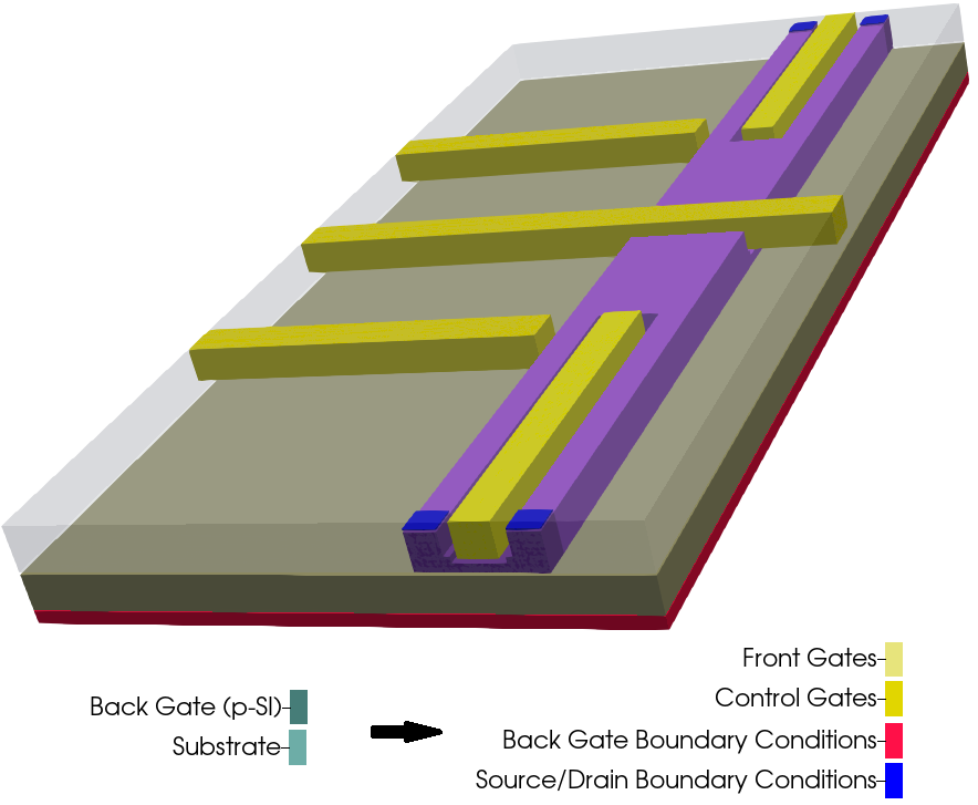
Figure 2.5.17.8 Regions substituted by adequate boundary conditions and final device representation
In 1D simulations it is required to choose the direction to be simulated that depends on the geometry of the specific device. In our example, the structure consists basically of a stack of layers where the Si layer is embedded, and is biased at the top and at the bottom. Then, a natural choice for 1D simulations of devices with this characteristic is along the growth direction that, by convention in nextnano++, is aligned in this case to the x-axis of the simulation system, as discussed before.
Depending on the complexity of the device it may be required to choose different points for the 1D simulations. Figure 2.5.17.9 illustrates some of these points that could be explored for the device of our example. From a quick analysis of our example we can observe that the line A is the most relevant for the first tuning of the grid, because it contains the most important coordinates of the interfaces to be examined.
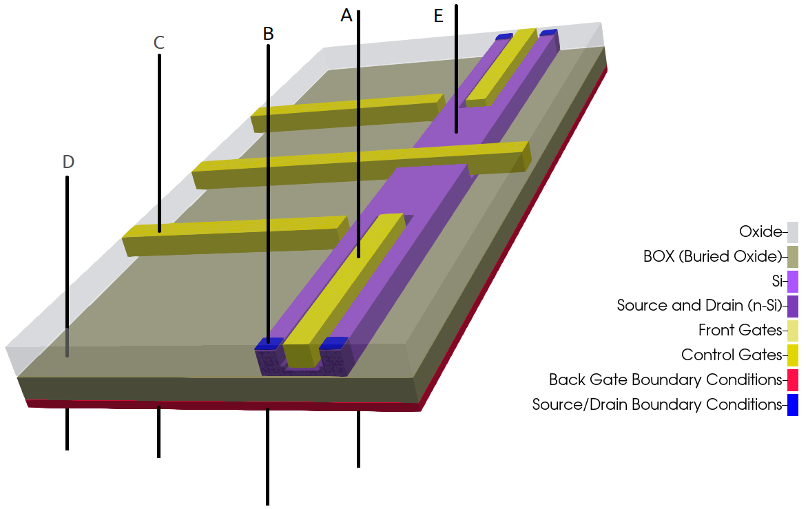
Figure 2.5.17.9 Representation of possible regions of study for 1D simulation in the growth direction.
The input file Large_device_simulation_1D_version_nnp.in presents the device as a stack of layers passing through one of the gates over the Si channel (line A). This can be used to set up and/or verify the parameters used to model each material of the structure. After simulation, we can easily identify, for example, the conduction band across this direction as shown in Figure 2.5.17.10.
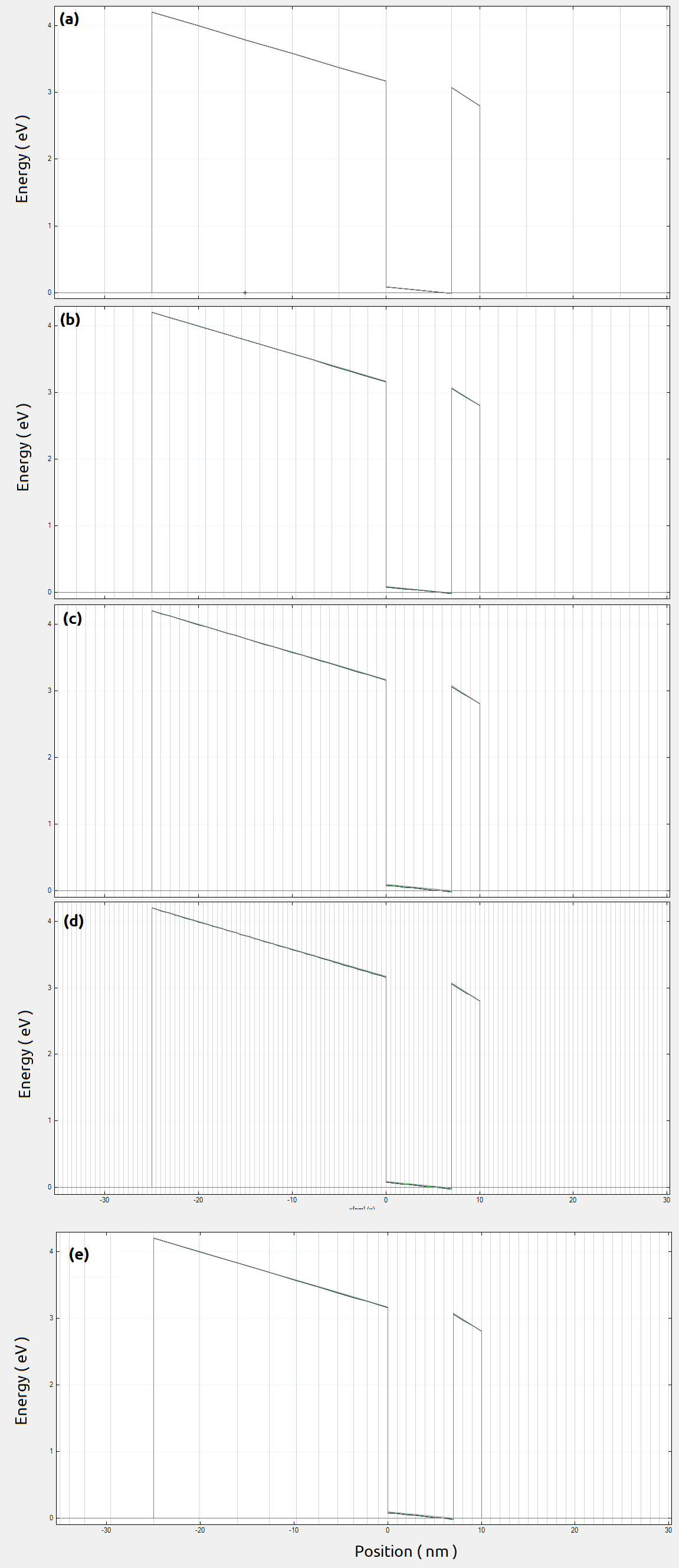
Figure 2.5.17.10 Conduction band resulting from 1D simulations in the growth direction along the line A for homogeneous grid resolution: (a) 5 nm, (b) 2 nm, (c) 1 nm and (d) 0.5 nm. The gray vertical lines represent the grid lines used in this simulation. (e) corresponds to a grid resolution of 1 nm inside the active region and 5 nm in the remaining parts of the structure ( in the growth direction ).
These plots were obtained by running this input file for different homogeneous grid line spacings in the growth direction ( from a to d ). We can easily identify the most important regions: the back-gate, the buried oxide, the channel ( surrounded by oxide ) and some of the top gates. Here, the most important region is the Si-channel ( the active region ), whose grid resolution can be increased.
Such input file runs very quickly, and it is a very good starting point for choosing a suitable grid resolution. From these plots we can observe that the conduction band is not too sensitive to the choice of the grid resolution in this direction. An ideal situation is to define a finer grid spacing in the active region and a coarse grid for the remaining parts of the device. It is recommended to make the final refining of the growth direction only in the last steps of the 2D or 3D grid tuning, for saving more runtime. In our example for the next simulations it will be used 1 nm and 5 nm grid as fine and coarse grid spacing for the growth direction, respectively ( plot e in Figure 2.5.17.10 ).
Hint
Visualize the grid lines selecting Simulation grid in nextnanomat menu.
Refining grid in 2D Simulations
Now it is time to perform the 2D simulations, using our input file Large_device_simulation_2D_version_nnp.in. It represents a slice of the device passing through the center of both front gates ( FGS and FGD ), parallel to the growth direction and the propagation direction, as shown in Figure 2.5.17.11.
This kind of representation can be very useful for defining the more convenient boundary conditions at equilibrium conditions for the gates and for the contacts. The device of our example requires these gates be modeled as highly-doped quasi-metallic regions at low temperatures. How to set them properly we invite you to visit our tutorial about contacts{}.
At this point we will freeze the grid resolution in the growth direction, and will refine the grid spacing along the propagation direction. In this way, when talking about grid resolution or spacing we will be referring to the propagation direction.
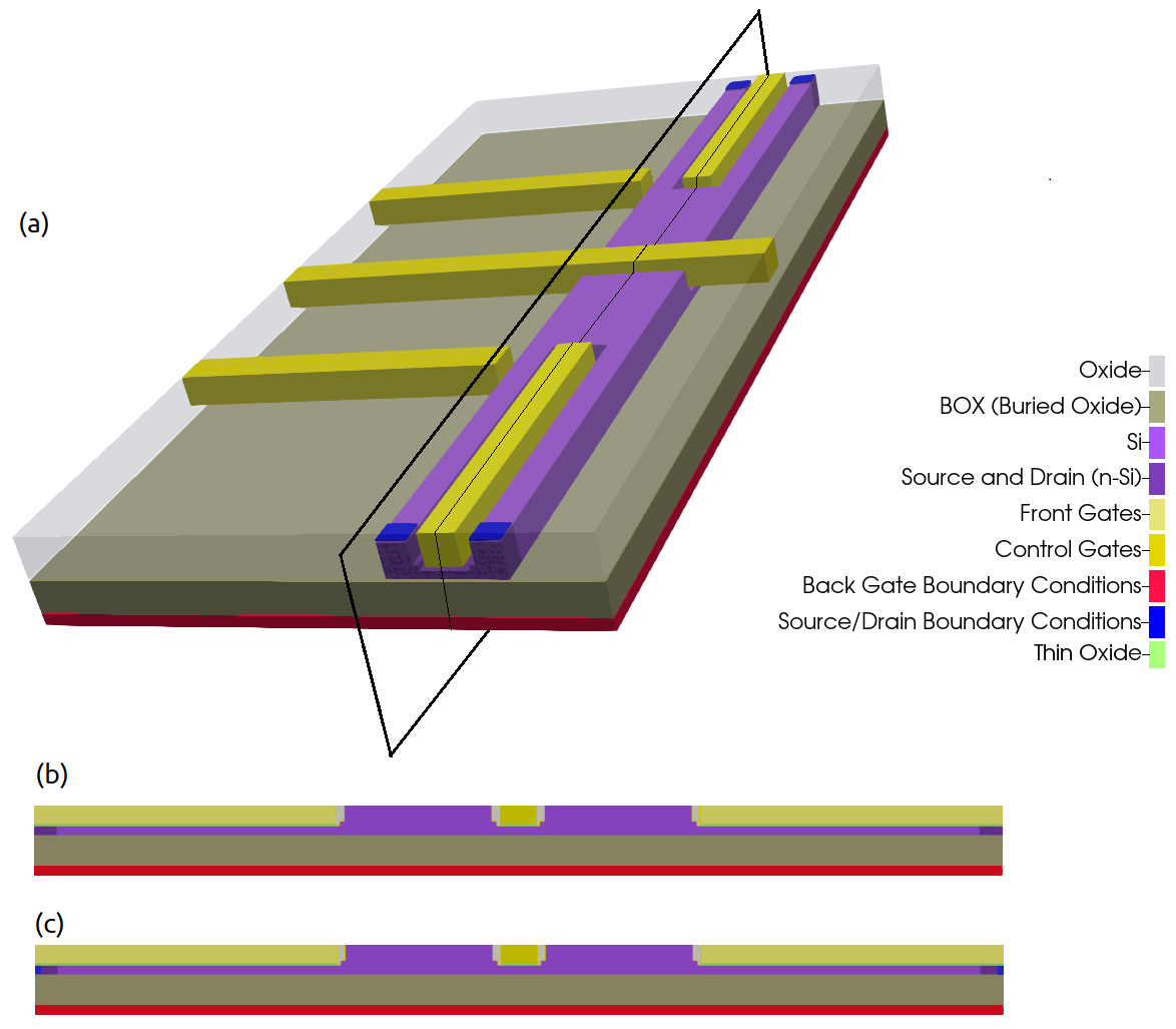
Figure 2.5.17.11 Slice simulated in our example.
Our main goal of these 2D simulations is the identification of the most important regions where the grid must be refined in the propagation direction. We will focus in the conduction band computed with different grid resolutions, that are presented in Figure 2.5.17.12. The data is stored in \bias_00000\bandedges.dat of the output folder.

Figure 2.5.17.12 Conduction band along a plane containing the growth direction and the center of the front gates. This result was obtaining grounding all gates and contacts, except the front gates that were biased at 0.8 V. The upper image corresponds to the full simulation domain simulated. The region inside the gray rectangle is presented below for different grid resolutions.
As soon we decrease the grid line spacing it becomes difficult to distinguish the results from the 2D plots. For this reason, it is recommended to include in the input file some 1D sections for both directions, that makes easier to compare the results. You will find several of these sections defined in the 2D input file of our example.
Hint
It is highly recommended to include the coordinates of all interfaces and the one used for specifying output sections and slices in the grid definition on your input file this avoids unnecessary interpolation of the results.
Figure 2.5.17.13 presents the comparison of the conduction band just 1 nm above the interface between the buried oxide and the Si-channel ( section xz_Si_2DEG of Figure 2.5.17.7 ) from 2D simulations with the different grid spacing.
The corresponding results can be found in the output files \bias_00000\bandedges_1d_xz_Si_2DEG.dat. From the image we identify that the central region from -150 and 150 nm at the most relevant for controlling the transit of carriers from one side to the other of the channel.

Figure 2.5.17.13 Conduction band at 1 nm above the interface between the buried oxide and the Si-channel ( section xz_Si_2DEG of Figure 2.5.17.7 ) from 2D simulations with the different grid spacing.
The gray lines correspond to the grid lines.
In Figure 2.5.17.14 we can observe in detail these regions for resolutions of 1, 5, 10 and 20 nm. The central region presents similar results using fine grids, while at the borders of the simulation region, a good model of the potential requires resolutions higher than 20 nm.

Figure 2.5.17.14 Comparison of the conduction band at a 1 nm above the interface between the buried oxide and the Si-channel ( section xz_Si_2DEG of Figure 2.5.17.7 ) from 2D simulations. The central region and the source contact regions are also shown with more details.
The first temptation is to use the minimum resolution as possible ( 1 nm ), but this is not necessary and not recommended: we have not started the 3D simulations yet. Figure 2.5.17.15 shows how the simulation time scales with the number of nodes and the grid resolution. We observe that for coarse grid ( grid line spacing around 20 and 100 nm ) the time for simulation does not change too much. Nevertheless, as soon it becomes fine the time starts to increase dramatically.

Figure 2.5.17.15 Runtime for 2D simulations as function of the number of nodes in the grid and the grid spacing.
A good strategy is to define different grid spacings in the x direction: small for the relevant regions ( central and the contact ) and larger for the ones that does not change ( the remaining ).
Last but not least, this simulation was performed for a specific combination of biases to the gates ( 0.8 V to the front gates, and 0 to the other gates and contacts ). It is not necessary to simulate all bias combinations, but it is useful to check some of them that can result in larger modifications of the potential at least in active region.
- Exercise:
Run the input file Large_device_simulation_2D_version_nnp.in for several grid resolutions and obtain the plot of Figure 2.5.17.15 for your system. All information required for this exercise ( number of nodes and runtime ) you can find in the file Large_device_simulation_2D_version_nnp.log in the output folder of each simulation.
Hint
The performance of the simulations can be improved setting the number of threads for a single simulation in the menu Tools >> Options >>
Simulation of nextnanomat.
It is also recommended to set the tab Tools >> Options >> Executable the command
-b <number the cores of your system>
as additional parameter passed to the executable (field Command line of this menu). For example, if you are a user of a 6- cores-processor, write
-b 6.
Using the grid defined in the growth and propagation directions, we can expand to the third dimension. The result is shown in the Large_device_simulation_3D_version_nnp.in that still we require further optimization, but with less effort.
We also recommend visiting our tutorials:
where we present another guidelines concerning efficient simulations of large devices in three dimensions.