Optimizing electrostatics simulation for big 3D designs
Attention
This tutorial is under construction
- Input Files:
Large_device_simulation_2D_version_nnp.in
Large_device_simulation_3D_version_nnp.in
Large_device_simulation_3D_version_reduced_nnp.in
- Scope of the tutorial:
Guidelines for refining the grid in 3D-input files
Performing electrostatic calculations efficiently
- Relevant output Files:
\bias_00000\bandedges_1d_xz_Si_QDs.dat
\bias_00000\bandedges_1d_yz_Si_QDs.dat
\bias_00000\density_electron_1d_xz_Si_QDs.dat
\bias_00000\density_electron_1d_yz_Si_QDs.dat
For structures that strain computations are not needed, obtaining the electrostatic potential is the first step even when more complex computations are required.
Nevertheless, self-consistent computations of the landscape potential with the charge distribution for large devices demanding high accuracy generally consume a huge amount of memory and long execution time.
This tutorial is the second part of a methodology for reducing the time in the development of the input files for modeling such 3D structures, that can be found in Approaching big 3D designs with Schrödinger-Poisson self-consistent solver. In this methodology we suggest to start by tuning the grid of the simulation using 2D versions of the correspondent 3D input file. Although it is not mandatory following this first step for implementing the suggestions in this tutorial, we strongly recommend its reading at Reducing dimensionality of 3D input files, for understanding of the main concepts also used here.
We will take as an example a structure that can be used in a semiconductor-based quantum computer, that we introduced in the first tutorial of the methodology and quickly summarized below.
Device to be simulated
Figure 2.5.17.16 presents a simplified version of a device found in the literature [Kriekouki2022] that consists basically of a 7 nm-Si layer buried in a silicon dioxide structure. This silicon layer corresponds to the channel where the quantum operations are performed.
The transport of the carriers depends on the combination of the voltage applied to the gates (FTS, FTD, LG1, LG2, LG3) at the top of the structure isolated from the silicon channel by a thin layer of oxide. At the bottom of the structure, just below the thick buried oxide layer, a back gate plays also an important role in the definition of the landscape potential. The source and drain contacts in this scenario act as the reservoirs that will provide the carriers that will propagate in the channel.
Applying adequate boundary conditions, the device to be simulated can be simplified as shown in the Figure 2.5.17.16 (shown in (b)).

Figure 2.5.17.16 Device to be simulated. The Si-channel is buried in the oxide. FTS, FTD, LG1, LG2, and LG3 at the top of the structure and the back-gate, between the thick oxide layer under of Si layer (BOX) and the substrate, are gates used to shape the electrostatic potential. Source and drain act as reservoirs of carriers propagating through the channel. Device (a) before and (b) after applying adequate boundary conditions.
Starting simulations in the semiclassical domain
The first thing we have to keep in mind is the goal of our simulation: which equations have to be solved, the accuracy we want to achieve, and other post-processing tasks that will be necessary. In our practical example is expected that under certain bias combinations a quantum dot is formed in the channel close to the lateral gates LG1 and/or LG3. Then, an accurate electrostatic potential self-consistently solved with the Schrödinger equation is required for obtaining a good estimate of the wave functions in the device, that will also be used in coherent transport calculations.
Nevertheless, self-consistent quantum computations with Poisson equation means that we need to a sufficient number of eigenvalues enough to reproduce the carrier densities that will be used in the next Poisson iterations. For this reason, the runtime of the whole simulation does not only scale with the number of nodes of the structure for the electrostatic potential calculations, but also depends on the size of the quantum region and the number of eigenvalues that has to be solved.
Then, as a general rule, setting the grid for 3D simulations is more efficient when started with semiclassical calculations, where only the Poisson equation, or even the coupled current-Poisson equations, is solved. Additionally, nextnano++ always uses the resulting potential as a first estimate for the next steps of the quantum computation and other calculations. As a rule of thumb, run and verify the results step by step. In other words, perform the next step of the computations when the previous step (the electrostatic problem) properly converged. In this tutorial we will focus only in the solution of the Poisson equation self-consistent with the semiclassical densities of electrons, for refining the grid of 3D input files. Hints for optimizing the performance of quantum simulations will be provided in a separated tutorial (Optimizing Schrödinger-Poisson self-consistent solver for electrostatic quantum dots).
Refining the grid of 3D-input files
It is more efficient following the first step of our methodology, where the grid is progressively refined in the growth and in the propagation directions, that results in the file Large_device_simulation_2D_version_nnp.in for 2D simulations. Then, it follows that the 3D version of this input file is simply the extension of the refined 2D version, that now includes the lateral gates LG1 and LG3 in the structure. The growth direction for 3D simulations is aligned to the z-axis of the simulation domain (see file Large_device_simulation_3D_version_nnp.in). Figure 2.5.17.17 shows the nomenclature of the most important points in the device coordinate system, sections and boundary conditions used in this input file.
It is clear that the previous grid tuning in 1D or 2D simulations is not a mandatory procedure: simultaneous tuning of the three axes in the 3D input file could be also performed. The disadvantage of this approach is that the execution time of each simulation depends on the number of nodes on the grid, that it is in higher number for the 3D case.

Figure 2.5.17.17 Device reference system and most important coordinates: (a) the 3D representation, (b) structure definition, and (c) structure after applying boundary conditions to the contacts and gates. Dotted lines (in red) represent sections defined in the input files.
Now it is time to start the simulations. Refining of the grid in the last dimension (x-axis) does not require, initially, high accuracy. In this way, the criteria that define the end of the convergence process (residuals, for example) can be “relaxed” in these first estimates. The idea is to identify regions of interest (ROI) where a fine grid has to be necessary to a suitable description of the density of electrons or holes in the simulated domain.
This is an iterative process where, looking at the conduction bands or the density of carriers in the ROI, we will try to refine the x-grid that the resulting density presents a smooth decay. For this task, it is recommended to define 1D slices in the most important ROIs and to overlay different plots in the same image within our graphical interface (nextnanomat). In our practical example, our objective it to capture the results in the region where the quantum dots are expected to be formed and different points where the density of carriers or the potential will be analyzed. Slices where the potential presents the steepest slopes are also important to be included in this analysis.
Figure 2.5.17.18 shows the conduction bands of two important ROIs, for a particular combination of biases (0.8V to both front gates, 4 V at LG1 and LG3, 1.7 V at the central gate (LG2) and 0 V for the remaining gates and contacts).
In the image, the xz_Si_QDs section corresponds to a slice at the region on Si-channel close to the interface with the gate LG1 (for x = 35 nm) and 1 nm above its interface with the buried oxide (BOX), where the quantum dot is expected to be formed. xz_Si_2DEG is the slice of the conduction band along the y direction at 1 nm below the oxide under the front gates (x = 0 nm).
Also important to observe is the slice yz_Si_QDs defined by the intersection of the plane along the longitudinal axis of the LG1 gate and the plane passing at 1 nm above the interface between the Si-channel and the BOX. These sections are shown in Figure 2.5.17.16 using dotted lines (in red).
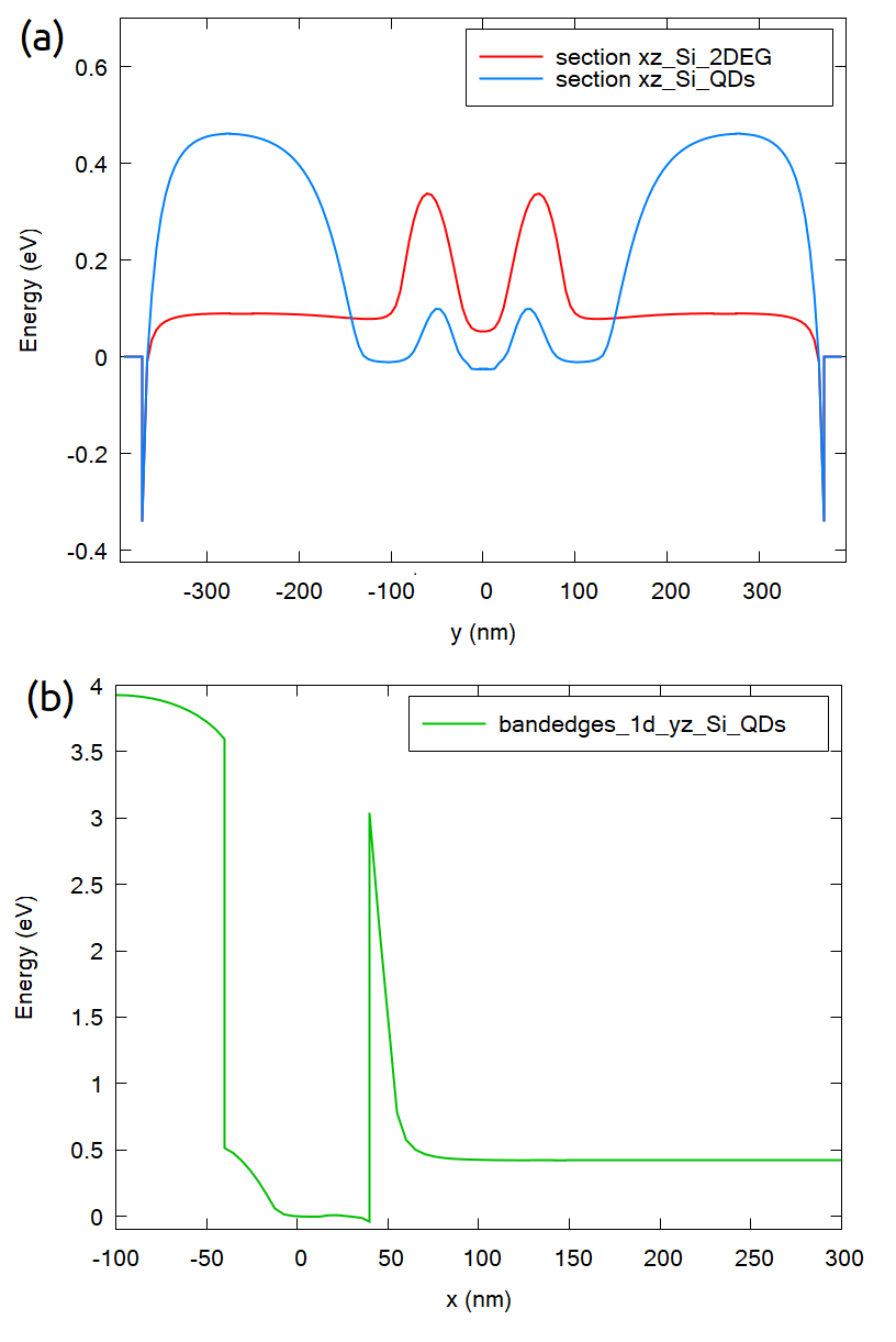
Figure 2.5.17.18 Slices of the conduction band in the two most relevant regions of interest for a particular combination of bias applied to the gates (see text):
(a) xz_Si_QDs, at 1 nm above the interface between the Si-channel and the BOX, close to the lateral gate LG1 (x = 35 nm), and xz_Si_2DEG, at 1 nm below the oxide under one of the front
gates (x = 0 nm), (b) yz_Si_QDs, at 1 nm above the interface between the Si-channel and the BOX, in the plane containing the longitudinal axis of the gate LG1.
The first step of the grid definition in the third axis consists in the elimination of unnecessary areas of the device. We need to distinguish two situations: solutions of quantum mechanics problems, or solutions of the electrostatics of the device only.
The first situation, when the semiclassical computations will be followed by computation of the wave functions, will demand more attention when eliminating or even reducing areas from the simulation domain. In this case we recommend that the final size of the device be defined only when the first quantum simulations be performed. A reduction of several undesired nodes at this moment still will bring benefits, but it is important a future evaluation of the impact of these cuts in the boundary conditions for the quantum calculations. Keep in mind that the wave functions can penetrate certain interfaces. Then preserve certain margin around the interfaces in order to allow a priori that some tail of the wave function can be properly calculated.
For the other situation, when we are only interested in the electrostatic solutions, this is the appropriate moment to cut these regions from the simulation domain.
Our particular example is in the first situation, and the elimination of some unnecessary areas can be valuable. We can expect a priori that the potential of the lateral gates LG1 and LG3 close to the Si-channel does not depend on the length of these gates, because of the large potential barrier between the Si-channel and the surrounding oxide of each gate, that practically results in vanishing of the wave functions at the interface of both materials. Then, this simplifies a lot our 3D simulations, because the lateral gates can be reduced and substituted by the convenient boundary conditions.
Figure 2.5.17.19 presents the impact of the changes of the lateral gate lengths on the results of the conduction band for the section xz_Si_QDs.
The results are practically equal, if the gate lengths are larger than 100 nm.
Then, we will use 100 nm as the length of the lateral gates for the reduced version of the 3D input file.
This value is also reasonable when we analyze the results for the section yz_Si_QDs (the growth direction), that practically independent of the choice of the level of this reduction.
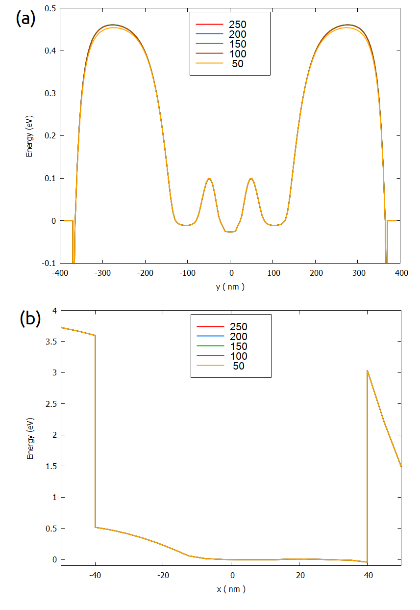
Figure 2.5.17.19 Conduction band in the quantum dot region as function of the length of the gates LG1 and LG3 in the simulation:
(a) slice xz_Si_QDs, and (b) slice yz_Si_QDs
Another natural candidate to be eliminated is the region from the start of the simulation system ($x_min = $x_4F).
Figure 2.5.17.20 shows the results of the conduction band for different values of $x_min, for the same slices of the previous image.
In this case, the extension of the negative axis of the simulation domain plays an important role in the definition of the electrostatic potential at the left border of the Si-channel (at x = -40 nm), while the region close to the lateral gates practically does not change (at x = 40 nm).
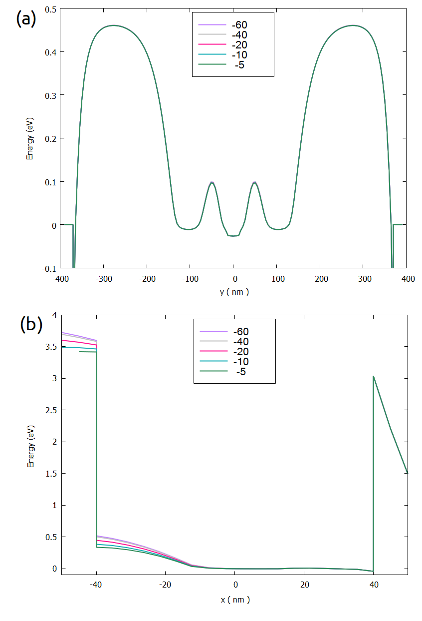
Figure 2.5.17.20 Conduction band in the quantum dot region as function of the value of $xmin:
(a) slice xz_Si_QDs, and (b) slice yz_Si_QDs.
Looking at to the conduction band results not enough to decide what it is an optimal value for $xmin to be used in the next simulations.
When this happens, more careful evaluation of the impact of these cuts have to be done.
Our suggestion is to verify the goals of the simulations and to combine results.
In our example, we can overlap to the conduction bands the corresponding density of electrons (our goal) and observe the differences using different cuts in the ROIs, as illustrated in the Figure 2.5.17.21.

Figure 2.5.17.21 Conduction band (dotted lines) and density of electrons (solid lines) in the xz_Si_QDs and yz_Si_QDs.
From this figure we can observe that in terms of electron density, they are not affected by the value of $x_min chosen. Similar analysis must be performed for all relevant results of the calculations.
Large_device_simulation_3D_version_reduced_nnp.in is the resulting input file after these reductions, and it will be used in the next computations. As we can observe, we are using a very conservative approach concerning the cuts around the Si-channel and the lateral gates, in order to give an example that would be done in a more general way.
If no quantum computations are necessary, this would be the moment of increasing the accuracy of the simulations by requiring lower residuals for the density and fermi levels, until the results (for example, density of electrons) does not change within a certain precision from one simulation to the other. If necessary, you can include some more lines in the positions of the grid for getting better results.
Once the grid is completely defined, make a final check concerning the sensitivity of the calculations with changes in the grid resolution.
Considerations if quantum computations will be required
Semi-classical computations of the density of electrons are very useful to identify how wide is actually the region where the carriers can be observed. Specially for self-consistent calculations, this evaluation is tremendously valuable because allows us to estimate the minimum size of the quantum domain to be simulated. It is always relevant to keep in mind that the total execution time in this case will also be affected by the number of the nodes in the quantum region and the number of eigenvalues to be used for self-consistent calculations, as we mentioned before. We will discuss in the more detail in our next tutorial of the presented methodology.
From Figure 2.5.17.21 we could identify the bounds of the region where most of the electrons are present. Then it is natural to choose them as first good estimate for the quantum region. Nevertheless, we must not forget that this result was obtained for one a specific combination of biases applied to the gates and the contacts. Then, it is convenient to make a quick check for some other combinations in order to verify if this region need to be extended.
Figure 2.5.17.22 shows the density of electrons overlapped with the respective conduction band for another bias combinations. Starting from the one presented above (0.8V to both front gates, 4 V at LG1 and LG3, 1.7 V at the central gate (LG2)), we changed either the bias on the back gate, in the central gate (LG2), or simultaneously in the other lateral gates (LG1 and LG3).
We can observe that applying bias to the back gate greater than 1.0 V, will require an extension of the quantum region from [-150, 150] to [-200, 200] in the y-direction.
Changes in the bias of the lateral gates does not change too much the semi-classical density of electrons distribution.
Then, in the next step we suggest to start defining the quantum region limited to the smaller interval ([-150, 150]), at least for the first setup of the input file including quantum calculations.

Figure 2.5.17.22 Conduction band (solid lines) and density of electrons (dotted lines) in the xz_Si_QDs sections changing only one of the bias of the combination discussed above:
(a) the back gate, (b) the central lateral gate (LG2), and (c) simultaneously to the lateral gates LG1 and LG3.
Here the full length of the lateral gate LG2 (250 nm) was used.
We also recommend visiting our tutorials:
where we present the first step of the methodology (the first one) and how to proceed for the case of the quantum calculations (the second one).