
GaN HEMT - semiclassical currents with low-field mobilities#
Last update: 2026-04-21
- Files for the tutorial located in nextnano++\examples\transistors
wz_III-N_GaN_HEMT_Dogmus_JPE_2018_1D.nnp(not available yet)wz_III-N_GaN_HEMT_Dogmus_JPE_2018_2D.nnp
This is an exemplary simulation of a nitride HEMT with a design similar to Fig. 1 (d) from [Dogmus2018]. The design heterostructure consists of, from bottom to top, AlN PVD layer, GaxIn1-xN buffer layer, GaN channel, and GaxIn1-xN barrier. Geometry of the gate is simplified and all the dimensions are reduced to make the simulation faster.
Note
While reducing the source-drain distance and size of the gate changes I-V and transfer characteristics, thinning the buffer and PVD layers down to single micrometers does not have much impact on the physics of this device.
Cu on the back side, Al gate, and TiN source and drain are modelled as perfect Schottky contacts with work functions of corresponding metals.
Insulation layer is modeled by an artificial wurtzite material with band gap, lattice parameters, dielectric constants, and selected effective masses describing Si3N4.
Remaining parameters are assumed to be irrelevant in this case.
Mobility of the GaN holding 2DEG has been artificially altered to give more realistic results.
For this purpose a material GaN_in_2DEG has been defined.
Here only Drift-diffusion and Poisson equations are solved self consistently including strain and piezo- and pyrolelectric polarization effects. Parabolic electronic energy dispersions are assumed. High-field mobility models are not used.
As hole currents are negligible, the hole densities entering the current equations are only limited to the values allowing the solver to successfully converge. By doing so, the hole current is not realistic. To provide that this limitation does not impact electron currents, the minimum and maximum hole densities are chosen in a range where changing them by an order of magnitude does not impact the solution much.
Attention
The simulation uses the default database parameters. Please review them before applying this simulation to your research.
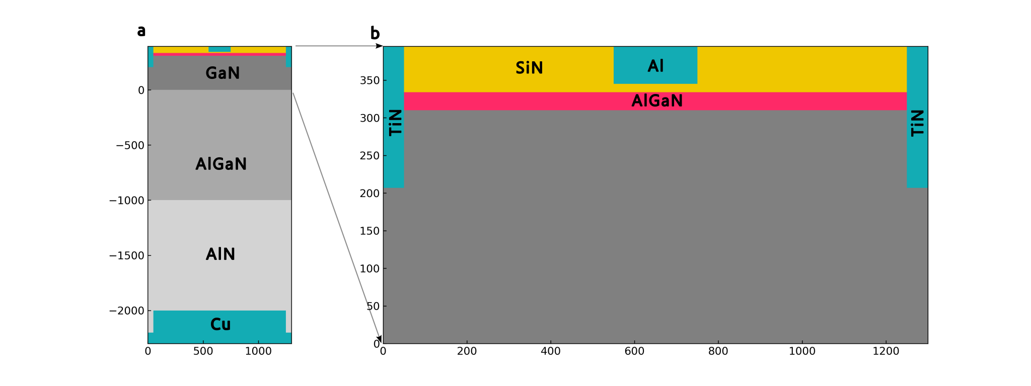
Figure 354 Regions as defined in the input file of a (a) full device (b) near the channel.#
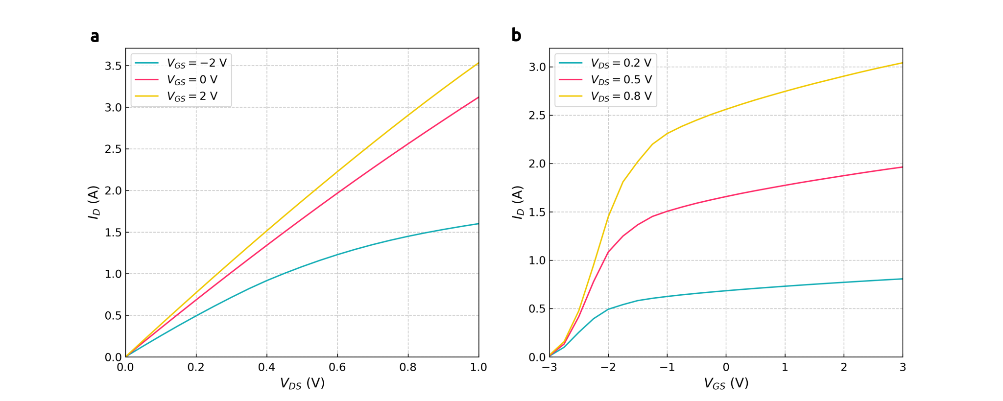
Figure 355 (a) I-V characteristics with VGS= -2, 0, and 2 V(b) transfer characteristics with VDS= 0.2, 0.5, and 0.8 V.#
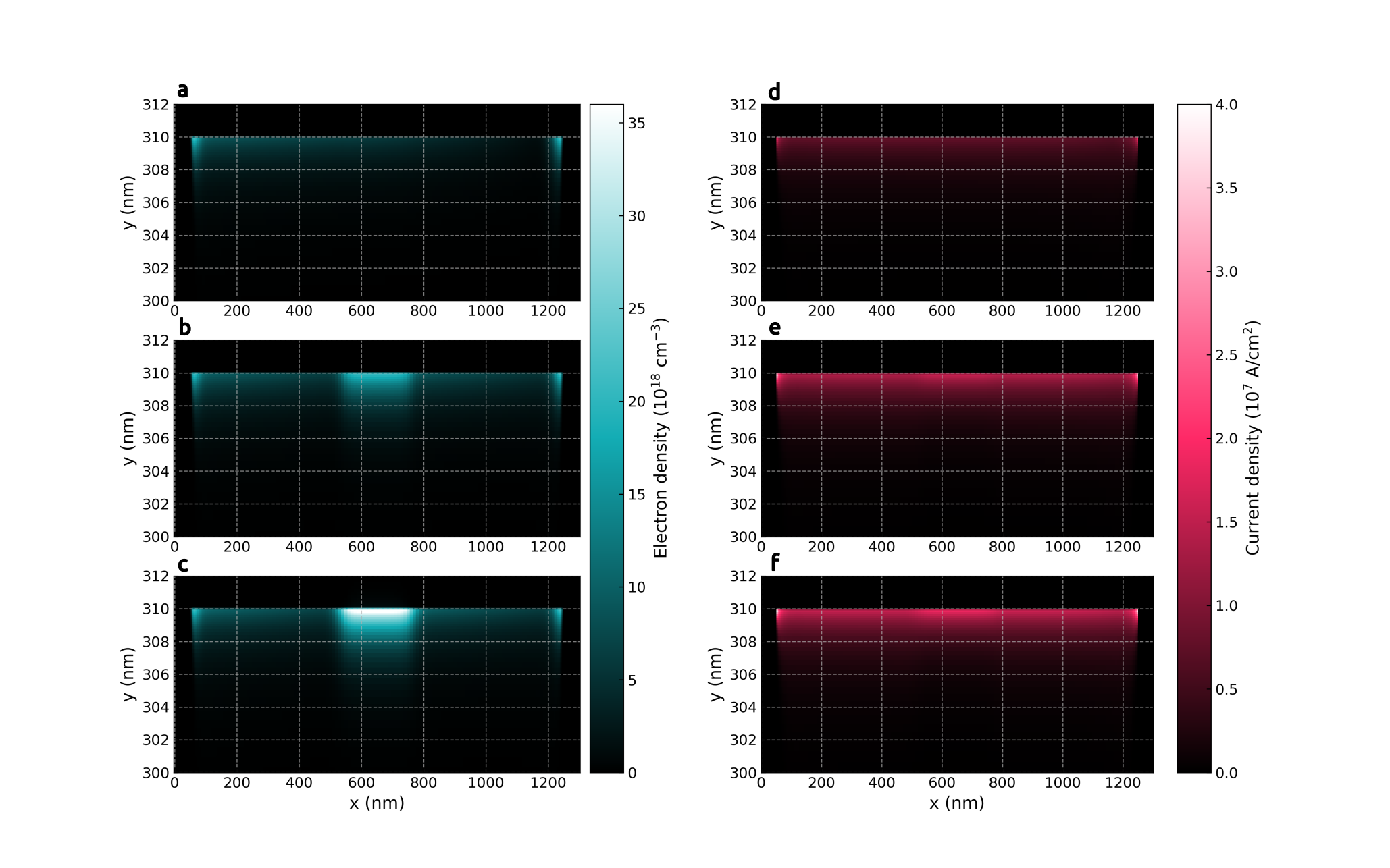
Figure 356 (a-c) Electron densities and (d-f) norm of the total current density with VDS= 0.8 and VGS= -2, 0, and 2 V.#
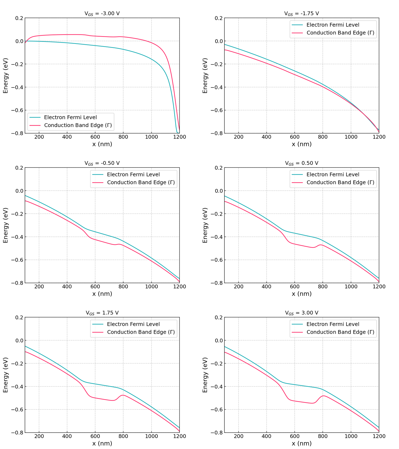
Figure 357 Section of the conduction band and electron quasi-Fermi level along the channel for VDS= 0.8 and various VGSfrom -3, up to 3 V.#
- Acknowledgment
This site is co-funded by European Union within the project CHIPS of Europe connecting universities and industry to train the next generation of semiconductor experts.