
T-shaped quantum wire grown by cleaved edge overgrowth (CEO): wave functions and strain#
Last update: 2026-04-27
- Files for the tutorial located in nextnano++\examples\quantum_wires
T-QWR_zb_III-V_Schuster_PhD_2005_1D_strained-QW.nnpT-QWR_zb_III-V_Schuster_PhD_2005_2D_strained.nnp
- Important output files
/Strain/hydrostatic_strain.fld(hydrostatic strain)/Strain/strain_*.fld(strain components)/Strain/density_piezoelectric_charges.fld(piezoelectric charge density)/bias_*/bandedges.fld(bandedge profiles)/bias_*/Quantum/probabilities_quantum_region_*.fld(wavefunctions)
Contents
Note
The tutorial is related to the PhD Thesis of R. Schuster [SchusterPhD2005]
Similar to the 1D confinement in a quantum well, it is possible to confine electrons or holes in two dimensions, i.e. in a quantum wire. In this tutorial we consider a quantum wire, which is formed at the T-shaped intersection of a 10 nm \(\mathrm{GaAs}\) type-I quantum well and a 10 nm \(\mathrm{In}_{0.16}\mathrm{Al}_{0.84}\mathrm{As}\) barrier. The T-shaped intersection is surrounded by \(\mathrm{Al}_{0.3}\mathrm{Ga}_{0.7}\mathrm{As}\) which acts as a barrier to GaAs. The \(\mathrm{In}_{0.16}\mathrm{Al}_{0.84}\mathrm{As}\) barrier has a larger lattice constant than \(\mathrm{Al}_{0.3}\mathrm{Ga}_{0.7}\mathrm{As}\) and is thus strained. The strain affects the GaAs well and thus produces a local decrease (increase) in the conduction (valence) band edge energy and thus confines electrons (holes) at the T-shaped intersection. The electrons and holes are free to move along the \(z\) direction only, thus, the wire is oriented along the [0-11] direction. Such a heterostructure can be manufactured by growing the layers along two different growth directions with the CEO (cleaved edge overgrowth) technique. Figure 431 shows the sample layout.
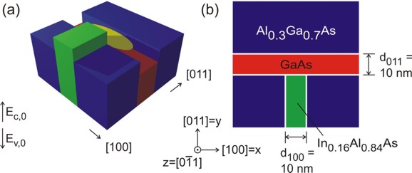
Figure 431 In (a) the two-dimensional conduction band edges of the T-shaped quantum wire without considering strain effects is shown. If one inverts the energy arrow then the left picture corresponds to the valence band edge. The wave function is indicated at the T-shaped intersection in yellow. In (b) a 60 nm x 60 nm extract of the schematic layout including the dimensions, the material composition and the orientation of the wire with respect to the crystal coordinate system is shown.#
It is useful to compare the structure above with the T-shaped quantum wire tutorial, which consists of two GaAs quantum wells rather than one GaAs well and one \(\mathrm{In}_{0.16}\mathrm{Al}_{0.84}\mathrm{As}\) barrier (see Figure 432), in order to understand the fundamental difference between these two layouts. As we see in from Figure 432 the wave function can extend into a larger volume as compared to the quantum well and thus reduces its energy. So quantum mechanics tells us that the ground state can be found at this intersection and electrons are only allowed to move one-dimensionally along the z direction. For Figure 431 however this is not true. The confinement only occurs if one takes into account the strain which decreases (increases) the conduction (valence) band edge energy in GaAs at the T-shaped intersection.
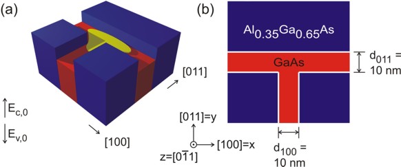
Figure 432 In (a) the two-dimensional conduction band edges of the T-shaped quantum wire (from the T-shaped quantum wire tutorial) without considering strain effects is shown. The wave function is indicated at the T-shaped intersection in yellow. In (b) a 60 nm x 60 nm extract of the schematic layout including the dimensions, the material composition and the orientation of the wire with respect to the crystal coordinate system is shown.#
Calculation of the strain tensor#
First, we have to calculate the strain tensor by minimizing the elastic energy within continuum elasticity theory. Along the translationally invariant \(z\) direction the lattice commensurability constraint forced the \(\mathrm{In}_{0.16}\mathrm{Al}_{0.84}\mathrm{As}\) layer to adopt the lattice constant of \(\mathrm{Al}_{0.3}\mathrm{Ga}_{0.7}\mathrm{As}\). The model for strain calculations can be specified inside the strain{ } group, where we choose the model: minimized_strain{ }.
In Figure 433 the calculated hydrostatic strain \(\epsilon_\mathrm{hyd} = \epsilon_{xx} + \epsilon_{yy} + \epsilon_{zz}\) (trace of the strain tensor) inside the structure is shown. The hydrostatic strain has its maximum at the intersection, where it leads to a reduced band gap, which is the requirement for confining the charge carriers. Thus, the quantum wire is formed in the \(\mathrm{GaAs}\) quantum well due to the tensile strain field induced by the \(\mathrm{In}_{0.16}\mathrm{Al}_{0.84}\mathrm{As}\) layer.
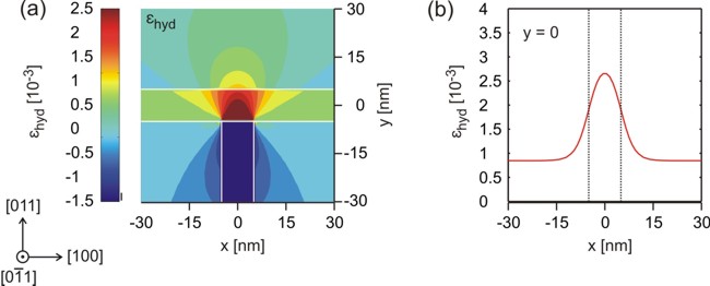
Figure 433 In (a) the hydrostatic strain \(\epsilon_\mathrm{hyd}\) inside the T-shaped quantum wire structure is shown. In (b) a cross-section of \(\epsilon_\mathrm{hyd}\) along \(x\) at \(y = 0\) is shown.#
Note that in a one-dimensional example, which is provided in the input file T-QWR_zb_III-V_Schuster_PhD_2005_1D_strained-QW.nnp, the strain tensor components of a \(\mathrm{In}_{0.16}\mathrm{Al}_{0.84}\mathrm{As}\) layer that is strained pseudomorphically with respect to an \(\mathrm{Al}_{0.30}\mathrm{Ga}_{0.7}\mathrm{As}\) substrate are the following:
Here, the growth direction is along the \(x\) direction, i.e. along [100]. The temperature is assumed to be \(40\,\mathrm{K}\) and the lattice constants are assumed to be temperature dependent (i.e. we use the \(40\,\mathrm{K}\) lattice constants).
In Figure 434 the individual strain tensor components (\(\epsilon_{xx}\), \(\epsilon_{yy}\), \(\epsilon_{xy}\)) with respect to the simulation coordinate system are presented. In our 2D simulation, the sample layout is homogeneous along the \(z\) direction, i.e. the lattice constant of \(\mathrm{In}_{0.16}\mathrm{Al}_{0.84}\mathrm{As}\) is forced to have the same lattice constant as \(\mathrm{Al}_{0.3}\mathrm{Ga}_{0.7}\mathrm{As}\) along the \(z\) direction. Then the strain tensor component must be \(\epsilon_{zz} = -12.4 \cdot 10^{-3}\), in agreement with our 1D example, i.e. \(\mathrm{In}_{0.16}\mathrm{Al}_{0.84}\mathrm{As}\), which has a larger lattice constant than \(\mathrm{Al}_{0.3}\mathrm{Ga}_{0.7}\mathrm{As}\) is strained compressively along the \(z\) direction. Similar to the 1D case, it is also expected that the \(\epsilon_{yy}\) component inside the \(\mathrm{In}_{0.16}\mathrm{Al}_{0.84}\mathrm{As}\) barrier has a similar value to \(\epsilon_{zz}\), which is clearly the case. The dark blue area in Figure 434 (c) thus has a value around \(-12 \cdot 10^{-3}\). However, this value deviates from the ideal 1D value at the T-shaped intersection as expected (see also Figure 435). The same applies to the value of \(\epsilon_{xx}\), which is similar to the 1D value inside the \(\mathrm{In}_{0.16}\mathrm{Al}_{0.84}\mathrm{As}\) barrier: \(\epsilon_{xx} = 11 \cdot 10^{-3}\). The strain tensor components \(\epsilon_{xz}\) and \(\epsilon_{yz}\) with respect to the simulation coordinate system are equal to zero as in our 1D example.
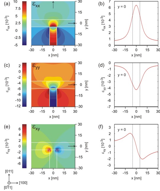
Figure 434 In (a), (c), (e) the strain components \(\epsilon_{xx}\), \(\epsilon_{yy}\), \(\epsilon_{xy}\) are shown. In (b), (d), (f) a cut through the structure along \(x\) at \(y=0\) is shown.#
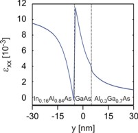
Figure 435 Strain tensor component \(\epsilon_{xx}\) along \(y\) direction at position \(x=0\).#
The important difference with respect to the 1D case is the existence of a non-vanishing strain tensor component \(\epsilon_{xy}\) which brakes the symmetry of the sample layout. Usually, the \(\epsilon_{xy}\) component is attributed to be responsible for piezoelectricity. However, note that in the discussion before all strain tensor components refer to the simulation coordinate system (and not to the crystal coordinate system). So we have to plot the off-diagonal strain tensor components that are expressed with respect the crystal coordinate system orientation and then check if the off-diagonal components are non-zero, which is clearly the case as we can see from Figure 436.
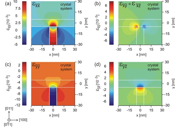
Figure 436 Strain tensor components \(\epsilon_{\tilde{x}\tilde{x}}\), \(\epsilon_{\tilde{y}\tilde{y}}\), \(\epsilon_{\tilde{x}\tilde{y}}=\epsilon_{\tilde{x}\tilde{z}}\) and \(\epsilon_{\tilde{y}\tilde{z}}\) with respect to the crystal coordinate system. The rotation with respect to the simulation system is a rotation of 45 degrees around the \(x\) axis, i.e. the [100] axis.#
By comparing Figure 434 (a) and Figure 436 (a) we observe that \(\epsilon_{\tilde{x}\tilde{x}} = \epsilon_{xx}\), because the \(x\) coordinate axes coincide. Symmetry arguments show that the following holds:
Calculation of the piezoelectric charge density#
The off-diagonal strain tensor components \(\epsilon_{\tilde{x}\tilde{y}}\), \(\epsilon_{\tilde{x}\tilde{z}}\) and \(\epsilon_{\tilde{y}\tilde{z}}\) are responsible for the piezoelectric polarization \(\mathbf{P}_\mathrm{piezo}\), given by
where \(e_{14}\) is the piezoelectric constant in units of \([\mathbf{C/m^2}]\). Once having determined the piezoelectric polarization, one is able to compute the piezoelectric charge density:
In Figure 437 the piezo electric charge density inside the quantum wire structure is shown. The strain-induced piezoelectric fields are then obtained from \(\rho_\mathrm{piezo}\) by solving Poisson’s equation.
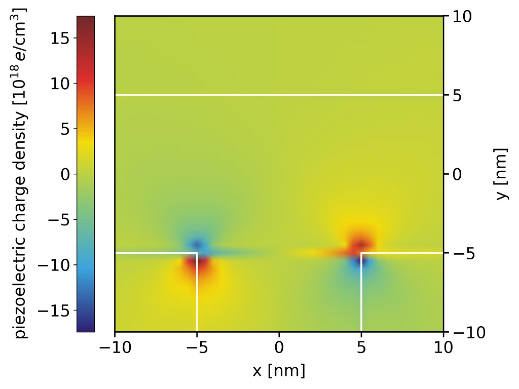
Figure 437 Piezoelectric charge density \(\rho_\mathrm{piezo}(x,y)\).#
Calculation of the conduction and valence band edges#
In Figure 438 the conduction and valence band edges of the structure are shown. The conduction and valence band edges were determined by taking into account the shifts and splittings due to the relevant deformation potentials as well as the changes due to the piezoelectric fields. We observe that the electron feels a conduction band minimum which is located left with respect to the T-shaped intersection. For the valance bands, we see that the valence band maximum for the heavy hole is not at the same position as the valence band maximum for the light hole.
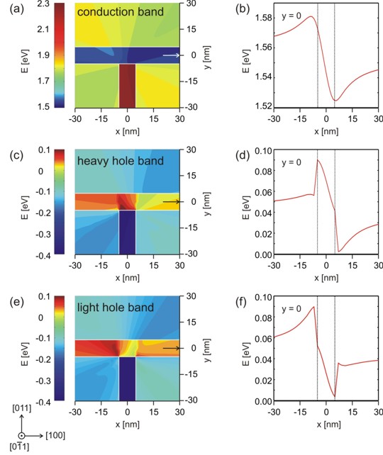
Figure 438 In (a), (c), (e) a 2D plot of the conduction, heavy hole and light hole band edge energies are shown. In (b), (d), (f) a cut through the conduction, heavy hole and light hole band edge energies at \(y=0\).#
Electron and heavy hole wave functions#
Figure 439 shows the square of the electron (e) and heavy hole (hh) wave functions (i.e. \(\psi^2\)). They were calculated within the effective-mass approximation (single-band).
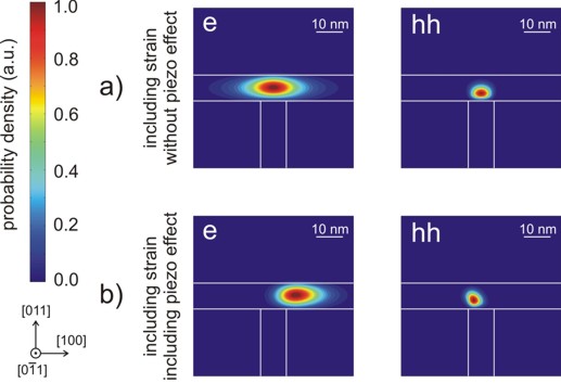
Figure 439 In (a) the contour diagram of the square of the electron (e) and heavy hole (hh) wave functions (i.e. \(\psi^2\)) for the case where strain is included in the simulations, but piezoelectricity is not. Subplot (b) shows the same results as in (a), but this time including the piezoelectric effect. Note that in the plot the wave functions are normalized so that the maximum equals one, respectively.#
In Figure 439 (a) the piezoelectric effect was not included. As one can clearly see in Figure 439 (b), the piezoelectric effect destroys the symmetry of the sample layout. The piezoelectric field results from the \(\epsilon_{xy}\) strain tensor component which is also not symmetric with respect to the T-shaped geometry.
- Acknowledgement:
We would like to thank Robert Schuster from the University of Regensburg for providing experimental data and some figures for this tutorial.