
InGaAs Multi-quantum well IRB-LED#
Last update: 2026-04-27
- Files for the tutorial located in nextnano++\examples
LaserDiode_InGaAs_1D_cl.nnpLaserDiode_InGaAs_1D_qm.nnp
Contents
Introduction#
In this tutorial, we simulate optical emission of a 1D InGaAs multi-quantum well LED grown on InP substrate. The blue region, seen in Figure 302, is the separate confinement heterostructure (SCH), which forms an optical waveguide in the transverse direction to confine the emitted light (red arrow). The multi-quantum wells and SCH are clad by InP on both sides. A voltage bias is applied to the gray edges.
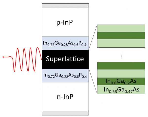
Figure 302 Structure overview#
Current equation#
The properties of optoelectronic devices are governed by Poisson equation, Schrödinger equation, drift-diffusion and continuity equations. We denote by \(n\) and \(p\) the carrier number density per unit volume. The continuity equations in the presence of creation (generation, \(G\) ) or annihilation (recombination, \(R\) ) of electron-hole pairs read
where the current is proportional to the gradient of quasi Fermi levels \(E_{F,n/p}(\mathbf{x})\)
Here the charge current has the unit of (area)\(^{-1}\)(time)\(^{-1}\). \(\mu_{n/p}\) are the mobilities of each carrier. In nextnano++, \(\mu_{n/p}\) are determined using the mobility model specified in the input file under currents{ }. Hereafter we consider stationary solutions and set \(\dot{n}=\dot{p}=0\). The governing equations then reduce to
which we call current equation (generation \(G=0\) in the present case). The nextnano++ tool solves this equation and Poisson equation self-consistently when one specifies it in the input file as:
run{
   current_poisson{ }
}
Recombination of carriers and emission spectrum#
The generation/recombination rate, \(R(\mathbf{x})\), originates from several physical processes. In nextnano++, the following mechanisms are implemented (cf. recombination_model{ } )
Schockley-Read-Hall recombination \(R_{\mathrm{SRH}}\) – carrier trapping by impurities.
Auger recombination \(R_{\mathrm{Auger}}\) – a collision between two carriers results in the excitation of one and the recombination of the other with a carrier of opposite charge.
radiative recombination \(R_{\mathrm{rad}}\) – emission/absorption of a photon.
Each mechanism can be turned on and off in the input file.
Radiative recombination describes the recombination of electron-hole pairs at a position \(\mathbf{x}\) by emitting a photon and is given by
where \(C(x)\) [\(\mathrm{cm}^3\mathrm{s}^{-1}\)] is the (material-dependent) radiative recombination parameter which is proportional to the one specified in the database (Net radiative recombination) and \(n(\mathbf{x}, E),p(\mathbf{x}, E)\) [\(\mathrm{cm}^{-3}\mathrm{eV}^{-1}\)] are the charge densities as a function of energy and position.
In nextnano++, this radiative recombination whose rate is calculated as above is regarded as spontaneous emission. On the other hand, the net amount of the stimulated emission rate is given by:
This is consistent with eq.(9.2.39) in [ChuangOpto1995]. We note that here it is assumed that photon modes occupied by one photon each, i.e. takes into account neither energy-dependent photon density of states nor Bose-Einstein distribution.
Since the radiative recombination process involves no phonons, this transition is vertical and therefore this contribution is only relevant for semiconductors with a direct band gap such as GaAs.
Absorption coefficient is calculated from \(R_{rad,net}^{stim}(E)\) as
where \(n_r\) is the refractive index and \(V\) is the total volume of the device. The unit is [cm\(^{-1}\)]. In case of 1D simulation, calculated \(R_{rad,net}^{stim}(E)\) has the unit [\(\mathrm{cm}^{-2}\mathrm{s}^{-1}\mathrm{eV}^{-1}\)] and is divided by the total length instead of the volume. This formula is consistent with eq (9.2.25) in [ChuangOpto1995].
Input file#
In the beginning of the input file, we define several variables for the structure and parameters for simulation. The variable definitions are shown in Figure 303.
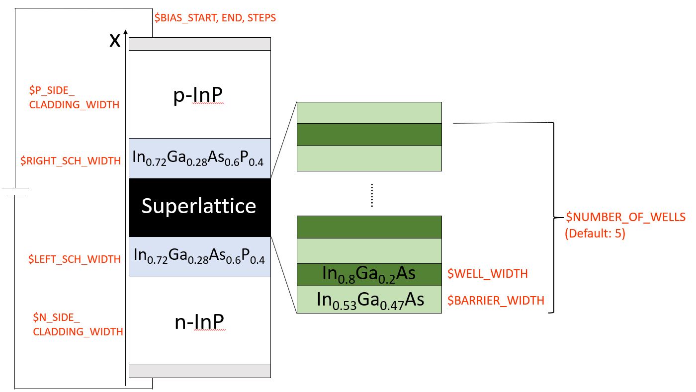
Figure 303 The definition of variables. The gray regions are contacts of 1nm thickness.
$NUMBER_OF_WELLS determines the repetition of quantum wells.
The program automatically sweeps the bias voltage starting from
$BIAS_START until $BIAS_END, at intervals of
$BIAS_STEPS.#
Charge density as a function of position \(n(\mathbf{x})\) is always calculated by default. On the other hand, charge density as a function of energy \(n(E),p(E)\), charge density as a function of both position and energy \(n(\mathbf{x}, E),p(\mathbf{x}, E)\) and emission spectrum are calculated when the followings are specified (see classical{ } for details):
grid{
    ...
    energy_grid{
        energy_min = -1.5                                  # Integrate from
        energy_max =  0.5                                  # Integrate to
        energy_resolution = 0.005                          # Integration resolution
    }
}


classical{
    ...
    energy_distribution{                                  # Calculation of carrier densities as a function of energy
        energy_min = -1.5                                  # Integrate from
        energy_max =  0.5                                  # Integrate to
        energy_resolution = 0.005                          # Integration resolution
        only_density_quantum_regions = yes
    }

    energy_resolved_density{
        only_density_quantum_regions = yes
        output_energy_resolved_densities{}
    }


    semiclassical_spectra{
        output_spectra{

            emission = yes
            gain = yes
            absorption = yes

            spectra_over_energy = yes
            spectra_over_wavelength = yes
            spectra_over_frequency = yes
            spectra_over_wavenumber = yes

            photon_spectra = yes
            power_spectra = yes

        }
        output_photon_density = yes
        output_power_density = yes
    }
}
The mobility model and recombination models for the current equation are specified in currents{ } as
currents{
    mobility_model = constant
#  mobility_model = minimos
    recombination_model{
        SRH         = yes          # 'yes' or 'no'
        Auger       = yes          # 'yes' or 'no'
        radiative   = yes          # 'yes' or 'no'
    }
}
The run{ } flag specifies which equations to solve.
This is the main difference between LaserDiode_*_qm.nnp and LaserDiode_*_cl.nnp.
# qm
run{
    strain{ }                                        # solves the strain equation
    current_poisson{                                # solves the coupled current and Poisson equations self-consistently
        output_log     = yes
        iterations     = 1000
        alpha_fermi = 0.5
    }
    quantum_current_poisson{                        # solves the Schrödinger, Poisson (and current) equations self-consistently
        iterations     = 1000
        alpha_fermi    = 0.9
        residual       = 1e6
        residual_fermi = 1e-8
        output_log     = yes
    }
}

# cl
run{
    strain{ }                                        # solves the strain equation
    current_poisson{                                # solves the coupled current and Poisson equations self-consistently
        output_log     = yes
        iterations     = 1000
        alpha_fermi    = 0.7
        residual_fermi = 1e-10
    }
}
In this case nextnano++ first solves the strain equation from the
crystal orientation to decide the polarization charges (piezoelectric
effect) and shifted band edges. Then the program solves the coupled
current-Poisson-Schrödinger equations in a self-consistent way (input
file: LaserDiode_InGaAs_1D_qm.nnp). For the classical calculation
(LaserDiode_InGaAs_1D_cl.nnp), quantum_current_poisson{ } is commented out to restrict the
calculation to the current-Poisson equations only.
Results#
Band structure#
The band structure and emission power spectrum of the system are stored in bandedges.dat.
Figure 304 shows the case for the bias \(0.2\) V.
Here the quasi Fermi level of electrons is lower than the quantum wells.
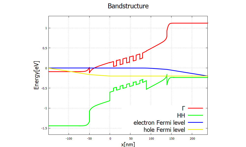
Figure 304 Band structure of the LED system for a low bias of \(0.2\) V.#
For the bias \(0.8\) V (Figure 305), in contrast, it lies above the red line,
allowing electrons to flow into the quantum wells.
An electron trapped in the quantum wells is likely to recombine with a hole in the valence band, emitting a photon.
In the output file bias_*OpticsSemiClassicallocal_emission_*.dat, one can see that the photons are emitted from this active region (not shown).
Figure 313 shows the emission spectrum in this case.
When the bias is too small, e.g. Figure 304, the intensity is much smaller, as can be seen in Figure 317.
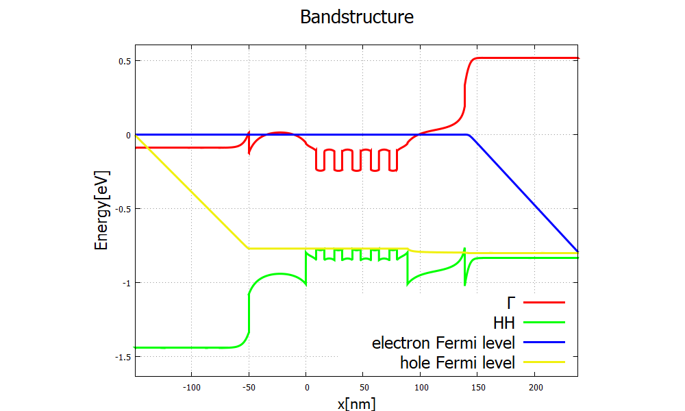
Figure 305 Band structure for a high bias \(0.8\) V. Electrons flowing from the left and holes from the right recombine in the active zone (multi-quantum well structure).#
Energy eigenstates and eigenvalues#
In the input file LaserDiode_InGaAs_1D_qm.nnp, the single-band Schrödinger equation is coupled to the current-Poisson equation and solved self-consistently.
The wave functions of electrons and holes along with eigenvalues are written in bias_*Quantumquantum_regionGammaprobabilities_shift_k0000.dat and bias_*Quantumquantum_regionHHprobabilities_shift_k0000.dat (Figure 306 and Figure 307).
The light hole and split-off states are out of the quantum wells and not of our interest here.
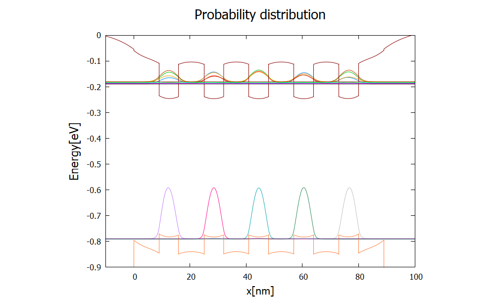
Figure 306 Probability distribution \(|\psi(x)|^2\) of the lowest localized modes of electrons and holes for the band structure Figure 304. Horizontal lines are the corresponding eigenenergies.#
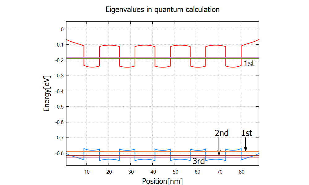
Figure 307 Eigenvalues of the Gamma-band up to 5th and heavy-hole-band states up to 13th in relation to band edges. The Eigenvalues above these are higher than the barrier energy of the quantum wells. The Gamma band has single “miniband”, whereas the heavy-hole band has three. The 1st heavy-hole miniband consists of the 1st~5th eigenvalues, the 2nd heavy-hole miniband consists of the 6th~11th eigenvalues and the 3rd consists of the 12th and 13th eigenvalues.#
Charge densities#
We can find the energy-resolved charge density \(n(x,E)\) and \(p(x,E)\) in the output bias_*electron_density_vs_energy.fld and bias_*hole_density_vs_energy.fld.
The following figures represent \(n(x,E)\) and \(p(x,E)\) [\(\mathrm{cm}^{-3}\mathrm{eV}^{-1}\)] with respect to the band edges and quasi-Fermi levels at bias 0.2, 0.4, 0.6, 0.8 and 1.0 V.
We can see that the carrier densities around the quantum wells increase as the bias increases.
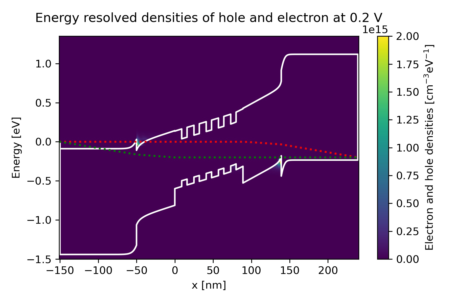
Figure 308 Energy-resolved electron and hole density, Gamma conduction band edge, HH valence band edge and quasi-Fermi levels at bias 0.2 V in quantum calculation.#
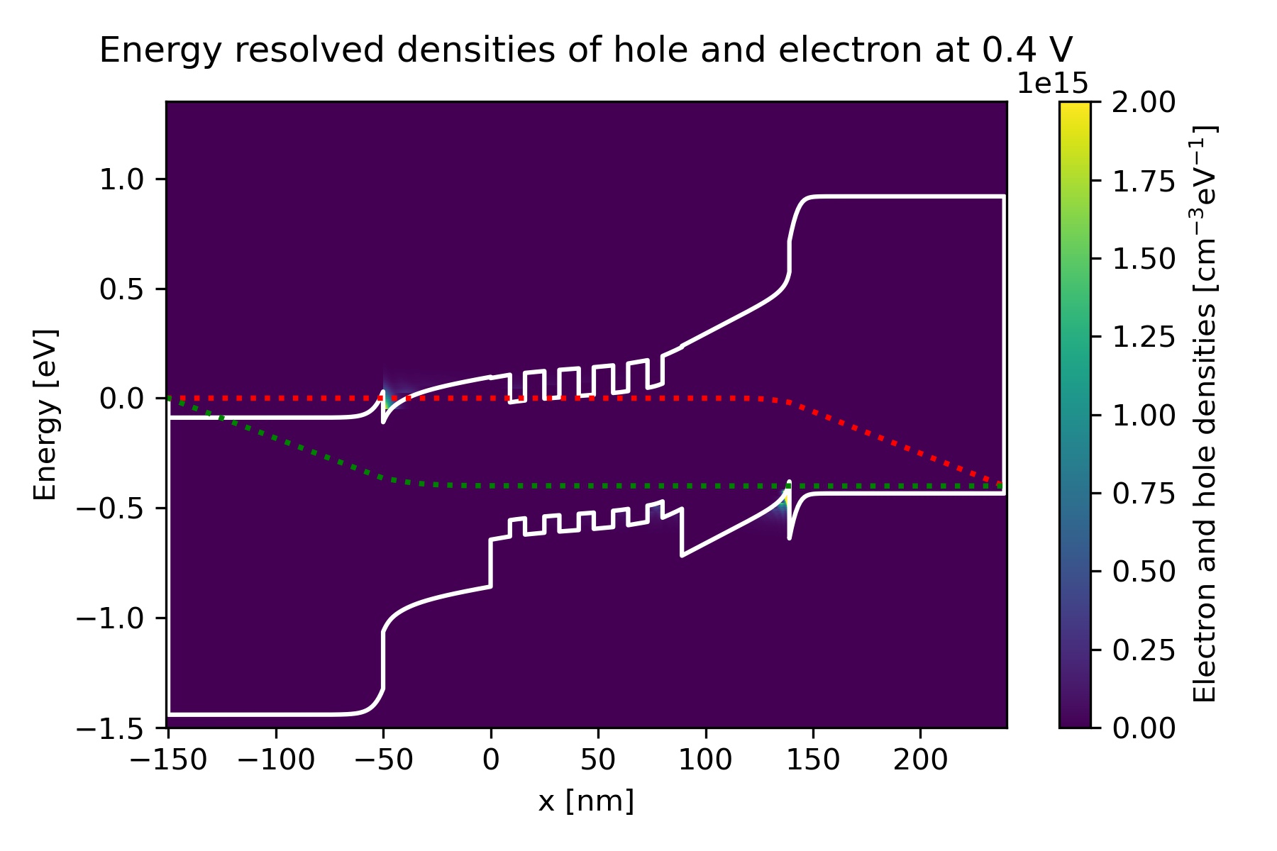
Figure 309 Energy-resolved electron and hole density, Gamma conduction band edge, HH valence band edge and quasi-Fermi levels at bias 0.4 V in quantum calculation.#
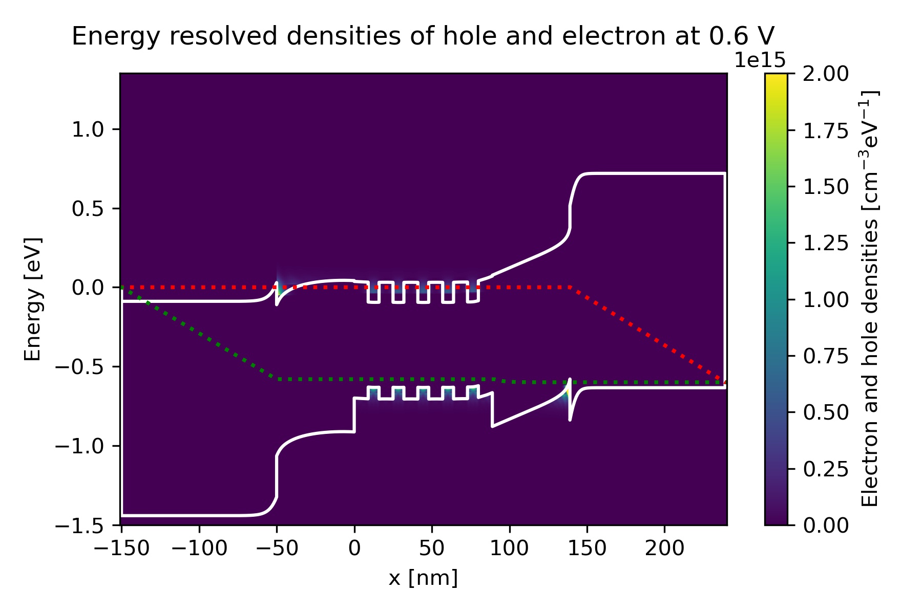
Figure 310 Energy-resolved electron and hole density, Gamma conduction band edge, HH valence band edge and quasi-Fermi levels at bias 0.6 V in quantum calculation.#
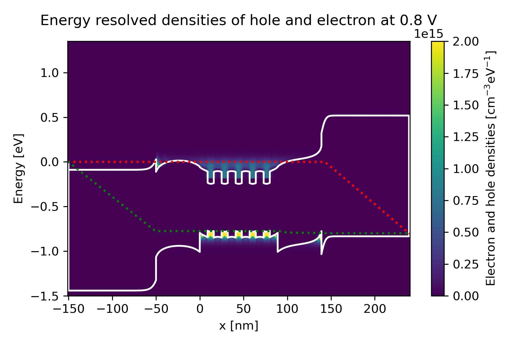
Figure 311 Energy-resolved electron and hole density, Gamma conduction band edge, HH valence band edge and quasi-Fermi levels at bias 0.8 V in quantum calculation.#
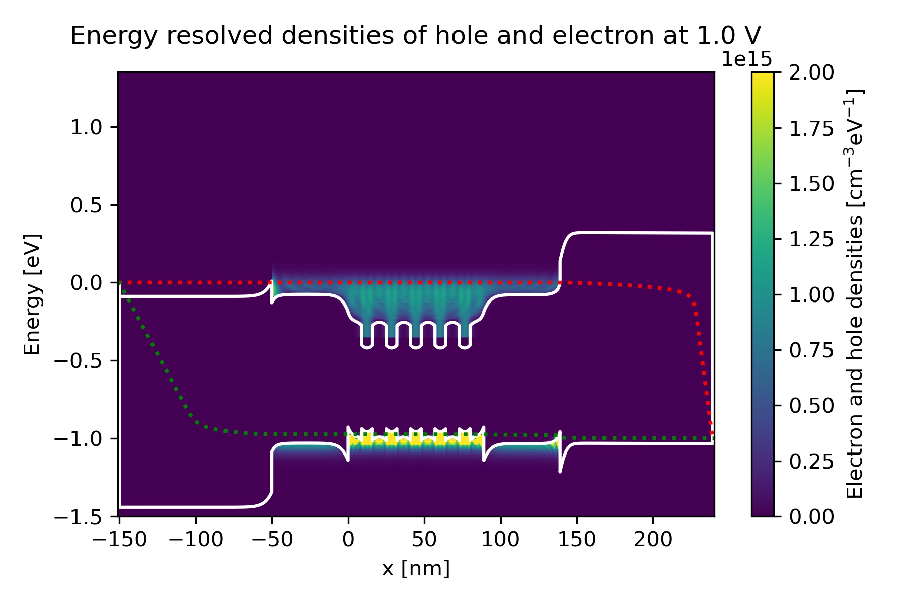
Figure 312 Energy-resolved electron and hole density, Gamma conduction band edge, HH valence band edge and quasi-Fermi levels at bias 1.0 V in quantum calculation.#
We also have the charge densities integrated over the device \(n(E),p(E)\) [\(\mathrm{cm}^{-2}\mathrm{eV}^{-1}\)] and energy \(n(x),p(x)\) [\(\mathrm{cm}^{-3}\)].
\(n(E)\) and \(p(E)\) with and without quantum calculation shows different features due to the discretization of energy levels in quantum wells.
This is shown in bias_*integrated_densities_vs_energy.dat.
Figure 313 illustrates the population inversion in stationary (quasi-equilibrium) state of the device under bias. Solid and dashed lines are for quantum and classical calculations, respectively. The black arrows mark the relevant energies of the structure 4 at bias of 0.8 V. The hole density is shown in Figure 314 with higher resolution.
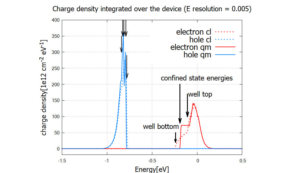
Figure 313 Electron (red) and hole (blue) densities integrated over the device as a function of energy.#
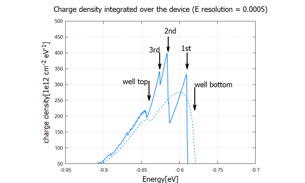
Figure 314 Hole density integrated over the device from classical (dashed) and quantum (solid) calculation.#
The energy resolution in Figure 314 has been increased by a factor of 10 from Figure 313.
Note
Although these charge densities either with variable \(E\) or \(x\) are both obtained by integrating \(n(x,E)\) and \(p(x,E)\) over the corresponding variable, these are independently calculated in nn++ simulation. Hence it is possible to turn off the calculation only for \(n(x,E)\) and \(p(x,E)\) calculating the integrated charge densities. In this case it runs much faster and needs much less memory.
Emission and absorption spectra#
The spontaneous emission spectrum is written in bias_*OpticasSemiClassicalspont_emission_spectrum_photons_*.dat (Figure 315).
The peak is at around 0.7-0.8eV, which is consistent with the charge distribution in Figure 313.
The formulas used for the calculation in the source code are specified above: Recombination of carriers and emission spectrum.
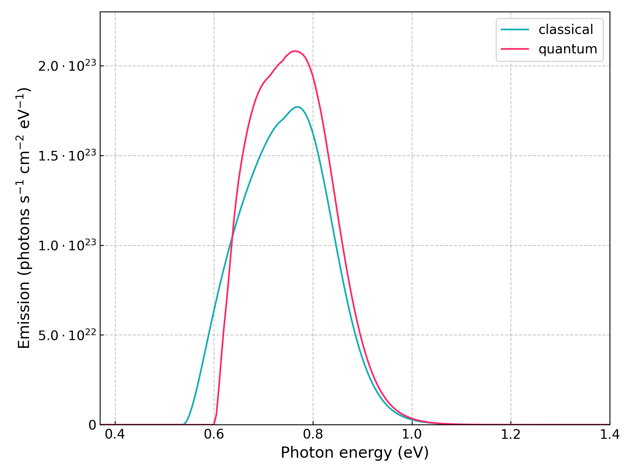
Figure 315 Emission spectrum of the LED for the bias \(0.8\) V.#
The absorption spectra are calculated as
where \(n_r\) is the refractive index and \(V\) is the total volume of the device. The unit is cm-1. In case of 1D simulation, calculated \(R_{rad,net}^{stim}(E)\) has the unit cm-2 s-1 eV-1 and is divided by the total length instead of the volume. This formula is consistent with eq (9.2.25) in [ChuangOpto1995].
The absorption spectra \(\alpha(E)\) and gain spectra \(g(E)\) are essentially the same quantity with opposite signs, with the constratint that the gain is only positively defined.
These are by definition independent of the initial photon population. Please note that the gain spectrum in nextnano++ is cut off where it is negative. For details, see classical{ }.
The spectrum changes its sign at the energy \(E_{Fn}-E_{Fp}\), that is,
the separation of the quasi Fermi levels. According to the output
bandedges.dat, this value is -0.0001-(-0.7702)=0.7701eV. The
following result has been calculated classically. We also get
qualitatively consistent results from quantum mechanical simulation.
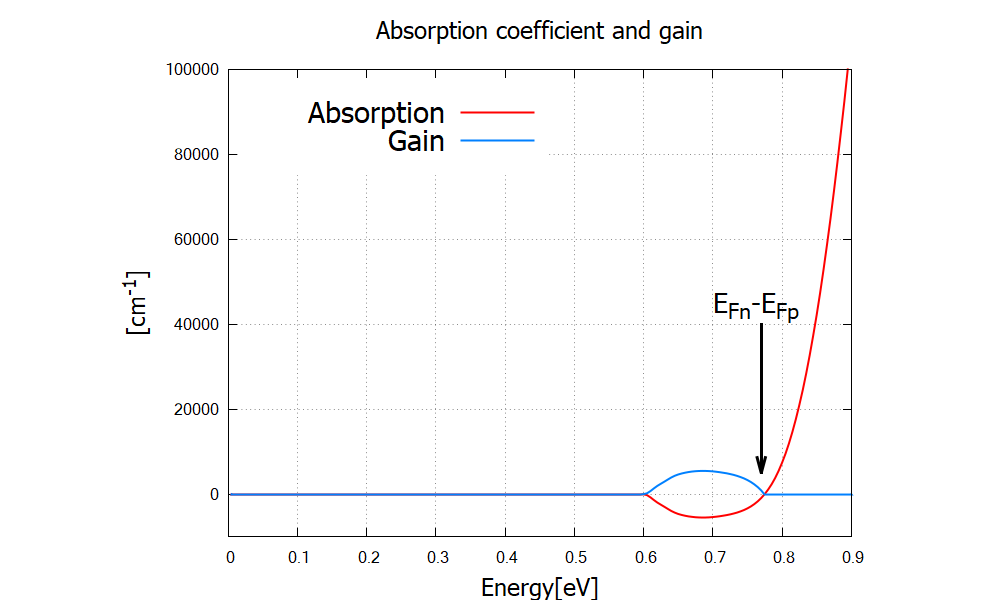
Figure 316 Classically calculated absorption and gain spectra. The sign of the spectrum switches at the energy corresponding to the quasi Fermi-level separation in the active region.#
Current and internal quantum efficiency#
The output file IV_characteristics.dat contains right- and left-contact current in unit of [Acm\(^{-2}\)].
In the present case, the right-contact current is hole current, whereas the left-contact current is electron current.
In Figure 316, we compare the hole current and photocurrent.
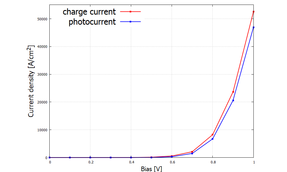
Figure 317 Charge current and photocurrent as a function of bias voltage (IV characteristics).#
Figure 317 clearly shows the consequence of the difference in band structures Figure 304 and Figure 305. The holes and electrons recombine in the multi-quantum well layers, emitting one photon per electron-hole pair. The efficiency of conversion from charge current into photocurrent is called the internal quantum efficiency (IQE).
The IQE values are written in bias_*emission_efficiency.dat and shown in Figure 318.
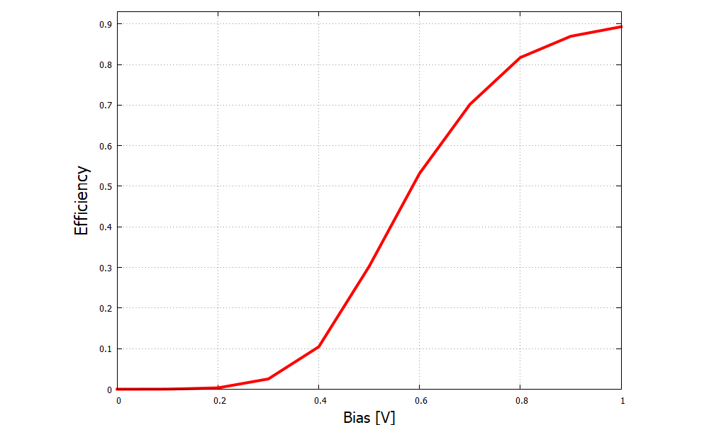
Figure 318 IQE of the InGaAs LED.#