

Electronic band structures of bulk crystals with 6, 8, 14 and 30-band k.p models#
Last update: 2026-04-21
- Files for the tutorial located in nextnano++\examples\electronic_band_structures
electronic-band-structure-all-kp-bulk_zb_IV_1D.nnp- Relevant keywords
- Important output files
bias_*/Bulk_dispersions/kp6/bulk_dispersion_L-G-X-W-K-L-W-X-K-G.datbias_*/Bulk_dispersions/kp8/bulk_dispersion_L-G-X-W-K-L-W-X-K-G.datbias_*/Bulk_dispersions/kp14/bulk_dispersion_L-G-X-W-K-L-W-X-K-G.datbias_*/Bulk_dispersions/kp30/bulk_dispersion_L-G-X-W-K-L-W-X-K-G.dat
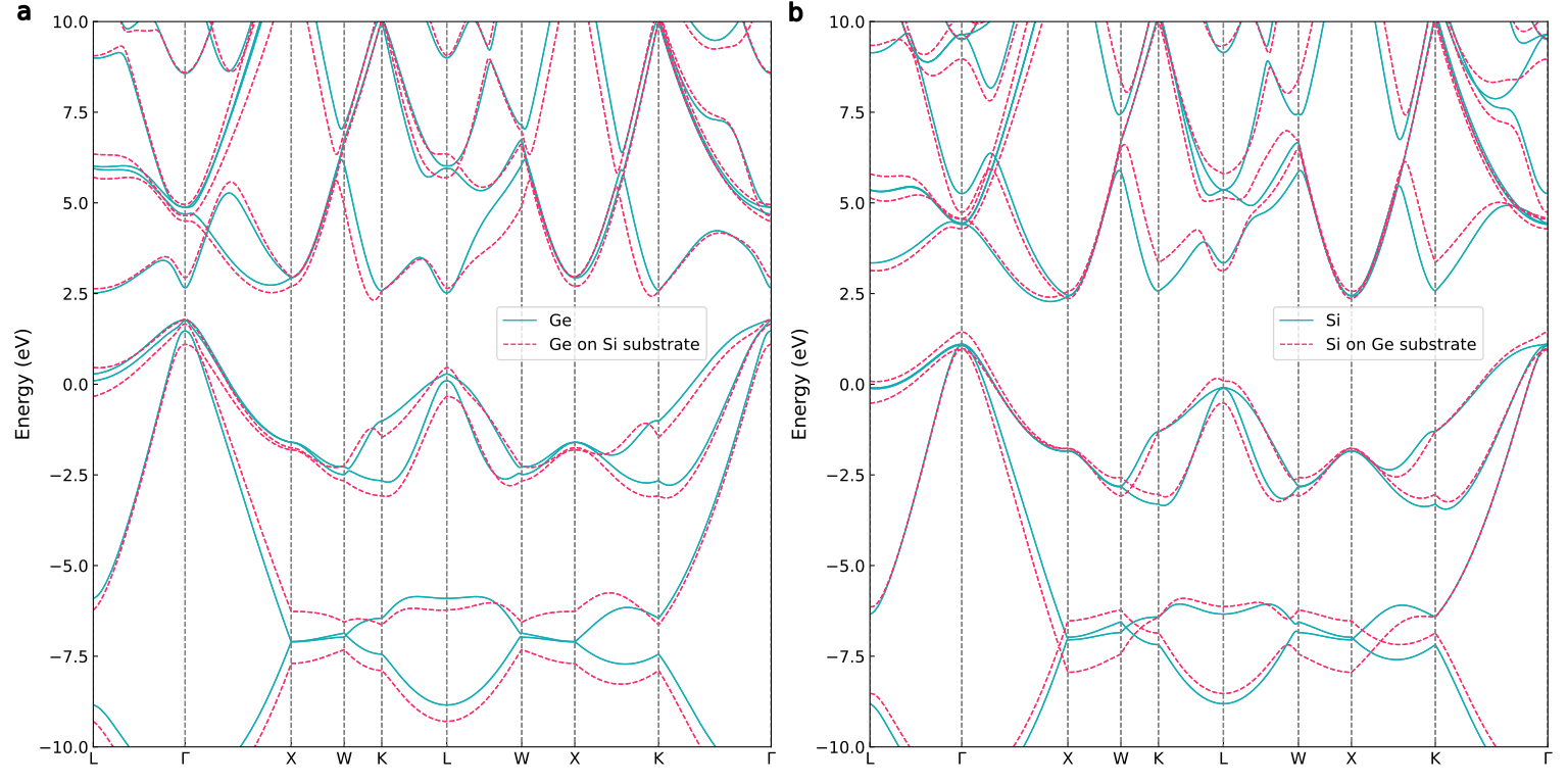
Figure 388 Electronic band structures calculated using 30-band \(\mathbf{k} \cdot \mathbf{p}\) method of (a) bulk Ge and strained Ge grown on (100) Si lattice; (b) bulk Si and strained Si grown on (100) Ge lattice.#
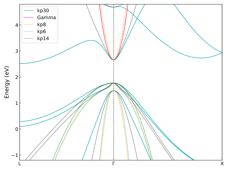
Figure 389 Comparison of electronic band structures of Ge obtained with various methods: 1-band for the conduction band, 6-band, 8-band, 14-band and 30-band \(\mathbf{k} \cdot \mathbf{p}\).#
- Acknowledgment
This page is based on the nextnano GmbH collaboration in the scope of the SiPho-G Project aiming at development of ultrahigh-speed optical components for next-generation photonic integrated circuits, and it is funded by the European Union’s Horizon 2020 research and innovation program under the grant agreement No 101017194.