

InAs/GaxIn1-xSb/InAs: triple quantum well#
Last update: 2026-09-09
Summary#
This example calculates the electronic band dispersion of an AlSb/InAs/GaxIn1-xSb/InAs/AlSb triple quantum well (TQW) using the 8-band \(\mathbf{k} \cdot \mathbf{p}\) method along a selected in-plane path and over a two-dimensional in-plane \(k\) grid. It also calculates control bulk 8-band dispersions in the barrier, outer-well, and central-well materials for reference.
Example information#
Files#
Physical system#
The heterostructure consists of a central 3 nm thick Ga0.7In0.3Sb quantum well surrounded on both sides by 10 nm thick InAs quantum wells and 5 nm thick AlSb barriers. The choice of materials results in a broken-gap (type-III) band alignment between the InAs and GaxIn1-xSb wells. Substrate material is set to AlSb so no strain is applied to the barriers. The temperature is set to 0.01 K.
Models and assumptions#
The confined states are calculated using the 8-band \(\mathbf{k} \cdot \mathbf{p}\) model parametrized with the Luttinger parameters. Solved Schrödinger equation uses Dirichlet boundary conditions at the two ends of the simulation domain. Strain effects are calculated using the pseudomorphic-strain model. The growth direction is set to [001].
Simulation setup#
As the structure is symmetric, it is defined centered at \(x=0\). The spatial grid is nonuniform. It is set the finest at the central layer and outer interfaces, and coarser in the outer wells and barriers. The grid spacings should be manually adjusted for different quantum-well thicknesses to ensure that the confined states are well resolved.
The electronic band structure is calculated from 0.4 nm-1 along \([001]\) direction, through the \(\Gamma\) point, until 0.4 nm-1 along \([011]\) direction and in the volume of the 2D in-plane \(k\) grid spanning from -0.4 to 0.4 nm-1 in both directions.
These two calculations are performed with the same grid spacing $dk = 0.02 nm-1 and can be triggered independently using the variable $_disp_full and $_disp_path.
Four electron states and two hole states are requested at each in-plane \(k\) point.
Integration over in-plane \(k\) space is disabled as the Poisson equation is not solved.
Three bulk 8-band dispersions for representative points in the barrier and both well materials are requested to provide the material context for interpreting the confined states in the TQW.
Negative effective masses are enabled explicitly to inform solver that it is expected for this material system. Output of probability densities is scaled up by a factor 5 to make them more visible in the plots.
Main functionalities of this simulation can be conveniently controlled using variables:
$_dispersion: when set to 1, quantum-well dispersion calculations are enabled,$_strain: when set to 1, pseudomorphic strain is included; when set to 0, it is disabled,$temperature: temperature expressed in K,$num_electrons: number of electron states requested,$num_holes: number of hole states requested,$Lx_barrier: thickness of each AlSb barrier,$Lx_QW_outer: thickness of each InAs outer quantum well,$Lx_QW_central: thickness of the central GaxIn1-xSb quantum well,$alloy_x_GaSb: Ga fraction in the central \(\mathrm{Ga}_{x}\mathrm{In}_{1-x}\mathrm{Sb}\) layer.Running the example#
Run the input file directly as provided.
Output files#
./bias_00000/bandedges.dat./bias_00000/Bulk_dispersions/kp8/bulk_dispersion_barrier.dat./bias_00000/Bulk_dispersions/kp8/bulk_dispersion_well_central.dat./bias_00000/Bulk_dispersions/kp8/bulk_dispersion_well_outer.dat./bias_00000/QuantumDispersions/well/kp8/dispersion_ky.dat./bias_00000/QuantumDispersions/well/kp8/dispersion_2D.fld./bias_00000/QuantumDispersions/well/kp8/probabilities_shift_k00000.dat./bias_00000/Quantum/well/kp8/spinor_composition_k00000_SXYZ.datResults#
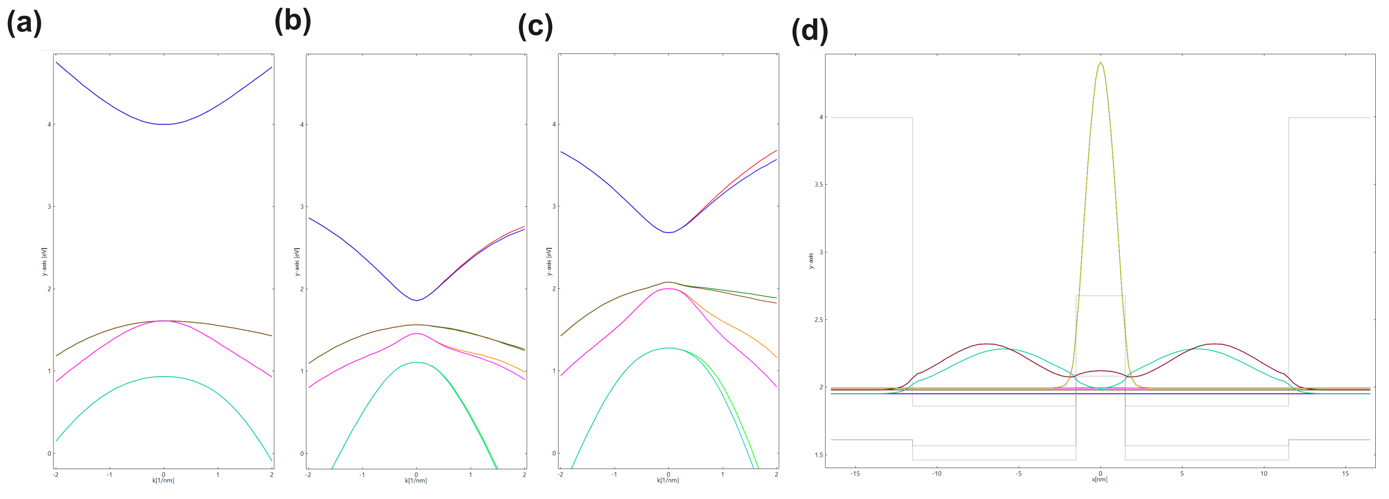
Figure 385 TEMPORARY FIGURE: Electronic band structures of bulk (a) AlSb barrier, (b) InAs outer well, and (c) GaxIn1-xSb central well calculated using 8-band \(\mathbf{k} \cdot \mathbf{p}\) method. (d) Energy profiles of two top valence bands and conduction band at \(\Gamma\) overlaid with probability densities of confined states.#
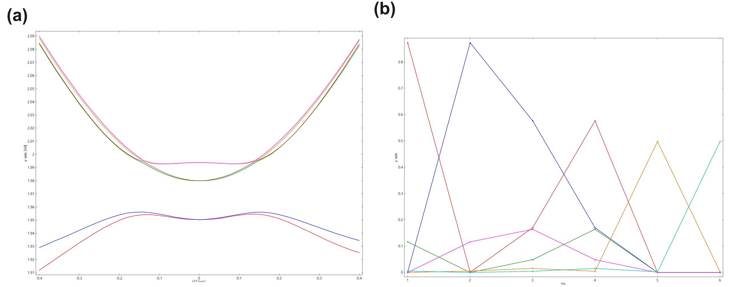
Figure 386 TEMPORARY FIGURE: (a) electronic band structure of the confined states along selected path, (b) Spinor composition of the confined states at \(\Gamma\), ordered from the lowest to the highest energy. Note that the states are double-degenerate at \(\Gamma\).#
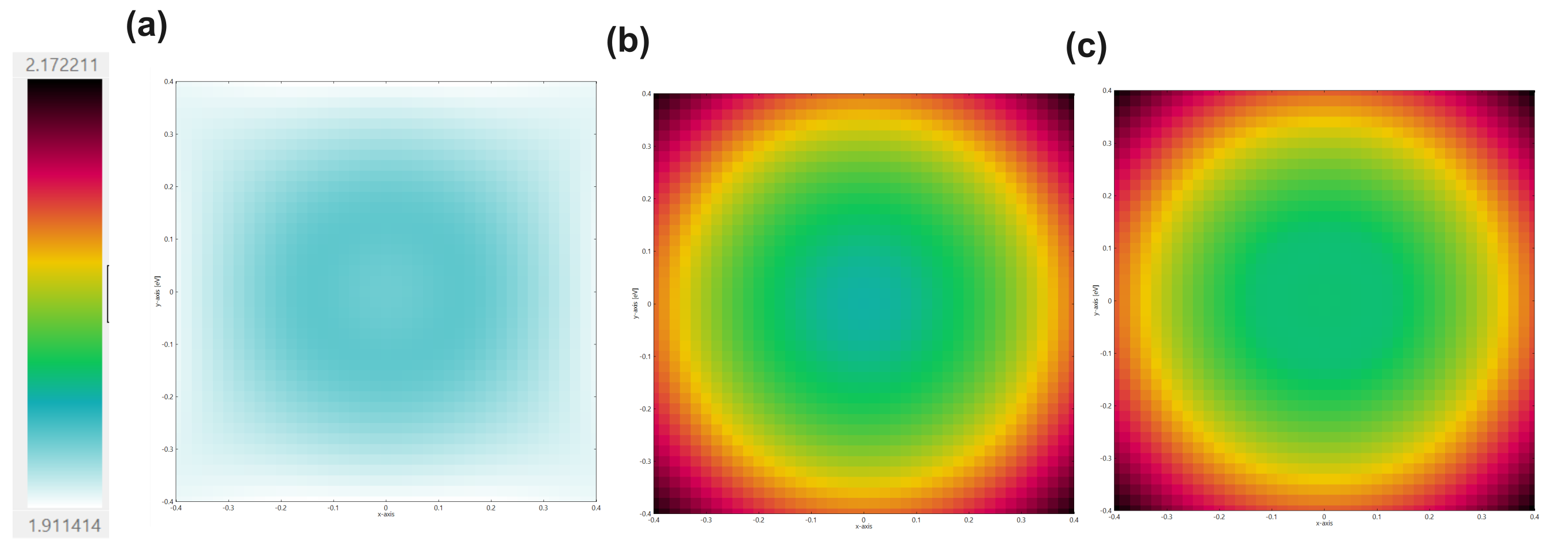
Figure 387 TEMPORARY FIGURE: Electronic band structure of the confined states on the 2D in-plane \(k\) grid for (a) 1st, (b) 3rd, and(c) 5th calculated quantized band.#