

InGaAs/AlInAs high-electron-mobility transistor#
Last update: 2026-04-21
- Files for the tutorial located in nextnano++\examples
HEMT_1D.nnpHEMT_2D.nnpHEMT_3D.nnp
Contents
Introduction#
This tutorial demonstrates how High Electron Mobility Transistors can be modelled with nextnano++.
HEMT structure#
Input file: HEMT_1D.nnp
The structure consists of the following material layers:
width [nm] |
material |
|
1 |
Schottky barrier 0.2 eV |
|
2 |
10.0 |
\(In_{0.532}Ga_{0.468}As\) |
3 |
25.0 |
\(Al_{0.477}In_{0.523}As\) |
4 |
50.0 |
\(In_{0.532}Ga_{0.468}As\) |
5 |
300.0 |
\(Al_{0.477}In_{0.523}As\) |
6 |
300.0 |
InP |
The conduction band edge profile without doping is plotted in Figure 358.
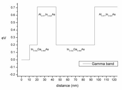
Figure 358 Calculated conduction band edge profile.#
Now we add at x = 35 nm a silicon delta doping of 4.5 \(\cdot\) 1012 cm-2 which leads to band bending. Instead of choosing a delta doping we specify a constant doping of 1.5 \(\cdot\) 1020 cm-3 that extends over 0.3 nm. (1.5 \(\cdot\) 1020 cm-3 \(\cdot\) 3 \(\cdot\) 10-8 cm = 4.5 \(\cdot\) 1012 cm-2)
We obtain two eigenstates and their corresponding wave functions inside the HEMT channel which leads to a two-dimensional electron gas (2DEG), see Figure 359. The electron density is plotted in blue.
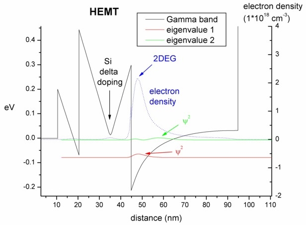
Figure 359 Calculated conduction band edge profile and probability densities.#
In the file bias_00000/total_charges.txt we can find the integrated electron and hole densities.
The total integrated density (from 10 nm to 100 nm) which can be measured experimentally is
1.87 \(\cdot\) 1012 cm-2 in agreement with the experiment.
Most of the density is located between 45 nm and 95 nm.
2D/ 3D simulations#
Input files: HEMT_2D.nnp, HEMT_3D.nnp
Input files for the same HEMT structure as in 1D, this time for a 2D and 3D simulations, are also available.
2D: rectangle of dimension 250 nm x 10 nm
3D: cuboid of dimension 250 nm x 10 nm x 10 nm