

HgTe/CdxHg1-xTe: topologically nontrivial simple quantum well#
Last update: 2026-08-04
Summary#
This example calculates electronic band dispersion of HgTe/CdxHg1-xTe simple quantum well by solving the Schrödinger equation using 8-band \(\mathbf{k} \cdot \mathbf{p}\) method, as well as eigenstates at the \(\Gamma\) point. It allows exploring phase transition of this quantum well CdxHg1-xTe from a trivial one to a nontrivial one depending on the alloy compositions and dimensions.
Example information#
Files#
quantum_well_CdHgTe_1d.nnp - complete input file for this examplePhysical system#
A single HgTe quantum well surrounded with CdxHg1-xTe barriers at 4.2 K.
Models and assumptions#
The example uses 8-band \(\mathbf{k} \cdot \mathbf{p}\) method with modified Luttinger parameters for both the electronic band structure and calculation of states in the quantum well at the \(\Gamma\) point. Strain effects are calculated using the pseudomorphic-strain model.
Simulation setup#
The quantum well is defined with its center at the x-coordinate 0. Grid lines are defined with 1 nm grid spacings at the simulation boundaries and 1/50 of the quantum-well thickness at the interfaces between the quantum well layer and the barriers. In this way lower, fixed resolution is set to the tails of the states, while providing good resolution in the quantum well itself, especially for very thin designs.
The electronic band structure is calculated from 2 nm-1 along \([011]\) direction, through the \(\Gamma\) point, until 2 nm-1 along \([001]\) direction. Negative effective masses are enabled explicitly to inform solver that it is expected for this material system. Substrate is set to CdxHg1-xTe with the alloy content equal to the material of barriers, hence no strain is present in the barriers.
Main functionalities of this simulation can be conveniently controlled using variables:
$strain: when set to 1 then strain effects are included, if set to 0 then otherwise$temperature: the temperature expressed in K,$alloy_x_well: alloy content \(x\) in CdxHg1-xTe of the well material,$alloy_x_barrier: alloy content \(x\) in CdxHg1-xTe of the barrier and substrate materials,$Lx_well: thickness of the well material$Lx_barrier: thickness of each barrierRunning the example#
Run the input file directly as provided.
Output files#
./bias_00000/bandedges.datenergy band profiles
./bias_00000/QuantumDispersions/well/kp8/dispersion_011_000_001.datelectronic band structure of teh quantum well
./bias_00000/Quantum/well/kp8/probabilities_shift_k00000.datprobability densiteis shifted to energies of the respective eigenstates
./bias_00000/Quantum/well/kp8/spinor_composition_k00000_SXYZ.datspinor composition at the \(\Gamma\) point
Results#
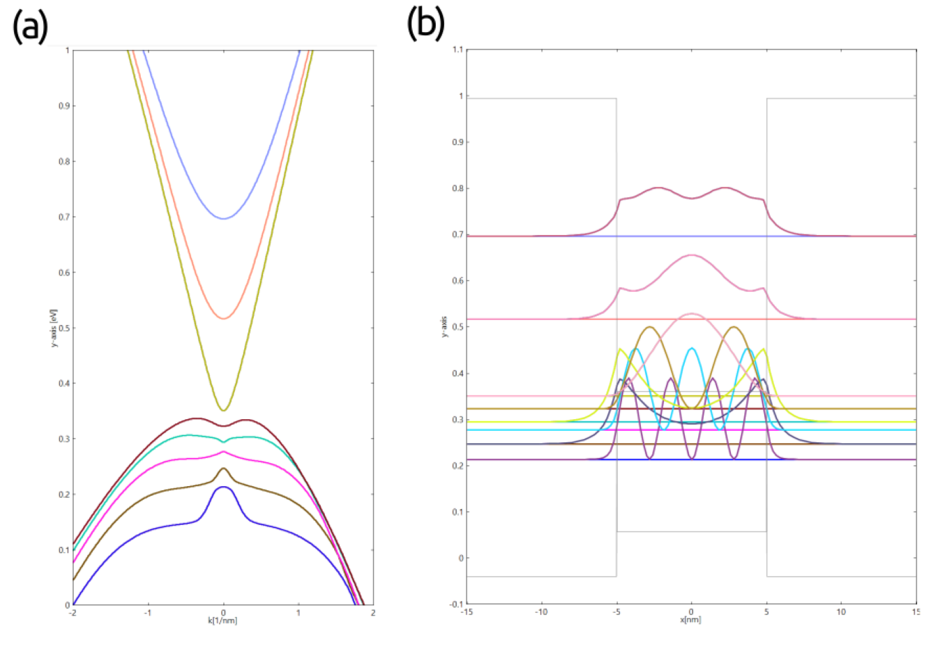
Figure 390 TEMPORARY FIGURE: (a) Electronic band structure, (b) energy profiles of two top valence bands and conduction band at \(\Gamma\) overlaid with probability densities of confined states.#
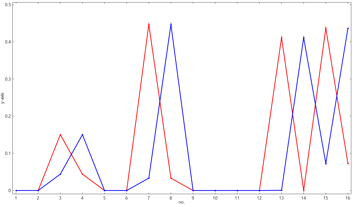
Figure 391 TEMPORARY FIGURE: Spinor composition of the confined states at \(\Gamma\), ordered from the lowest to the highest energy. Note that the states are double-degenerate at \(\Gamma\).#