

Electrostatically defined quantum dot#
Last update: 2026-04-21
- Files for the tutorial located in nextnano++\examples
SET_Scholze_IEEE2000_1D_nnpp.nnpSET_Scholze_IEEE2000_3D_cl_nnpp.nnpSET_Scholze_IEEE2000_3D_top_gates_cl_nnpp.nnp
Contents
Introduction#
In this tutorial, we simulate an \(AlGaAs\)/ GaAs heterostructure grown along the z direction. The tutorial is based on [Scholze2000]. The \(AlGaAs\)/ GaAs heterostructure leads to a two-dimensional electron gas (2DEG). By applying a gate voltage on top of the structure in the (\(x\), \(y\)) plane, one is able to deplete the 2DEG and a laterally defined QD is formed. By adjusting the gate voltage, one is able to tune the number of electrons that are inside the QD.
Figure 512 shows the conduction band edge \(E_\mathrm{c}\) (\(x\), \(y\)) and the electron density \(n(x,y)\) for the 2DEG plane, i.e. at \(z\) = 8 nm below the GaAs/ \(AlGaAs\) heterojunction.
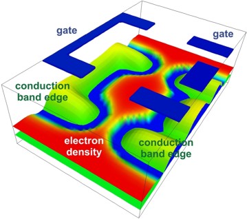
Figure 512 Conduction band edges (green), electron density (red) and geometry of the top gates (blue).#
We divide the tutorial into two parts:
In part 1, we simulate the heterostructure along the \(z\) direction and neglect the gates. (1D simulation: self-consistent Schrödinger-Poisson equation),
SET_Scholze_IEEE2000_1D_nnpp.nnp
In part 2, we solve the 3D Poisson equation to study the effect of the gates. (3D simulation: only Poisson equation using a classical density),
SET_Scholze_IEEE2000_3D_top_gates_cl_nnpp.nnp
Part 1: 1D simulation (self-consistent Schrödinger-Poisson)#
Figure 513 shows the calculated conduction band edge and the electron density of the heterostructure. The results are similar to Fig. 4 in [Scholze2000].
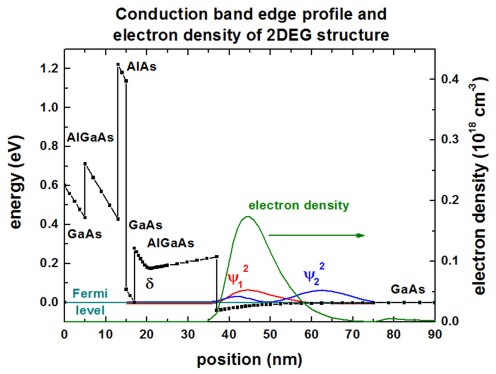
Figure 513 Conduction band edge profile (black), electron density (green) and Fermi levels (cyan) of 1D simulation.#
At the left boundary, a Schottky barrier of 0.6 V has been assumed. At \(z\) = 20 nm, a \(\delta\)-doping layer is present. The Fermi level is assumed to be constant at \(E_\mathrm{F}\) = 0 eV. The ground state wave function (\(\Psi_1\)) is ~8 meV below the Fermi level and dominates the electron density. The first excited state (\(\Psi_2\)) is ~3 meV above the Fermi level, the second excited state (not shown) is 19 meV above the Fermi level.
Part 2: 3D simulation with top gates (Poisson equation only)#
Figure 514 shows the 3D structure that we are going to simulate.
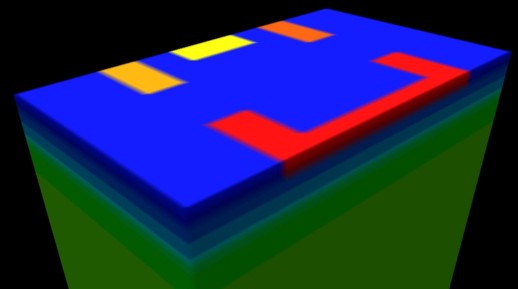
Figure 514 Device structure (3D)#
Figure 515 shows two 2D slices through the lateral \((x,y)\) plane at a distance of 8 nm below the \(AlGaAs\)/ GaAs interface. The results are similar to Fig. 5 in [Scholze2000]. At the top, the four gates are shown.
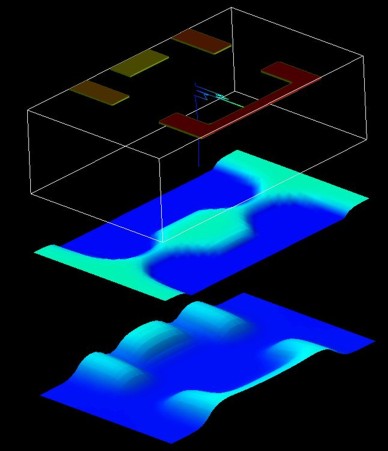
Figure 515 In the middle, the electron density is shown. The electron density has been calculated classically. At the bottom, the conduction band edge is shown.#