

Electronic band structures and phase transition in CdxHg1-xTe-based modulation-doped quantum well#
Last update: 2026-06-03
- Available for our customers upon request.
zb_II-VI_CdHgTe_QW_PRB_Novik_2005_1D.nnpzb_II-VI_CdHgTe_QW_PRB_Novik_2005_1D.py
- Main adjustable variables
$NUME,$NUMEnumber of states in conduction (electron) and valence (hole) bands (needed for the \(\mathbf{k} \cdot \mathbf{p}\) model);
$TEMPtemperature (K);
$x_alloy_wellpercentage of Cd in the CdxHg1-xTe alloy
$QW_width,$BARRwidth of the quantum well and barriers (nm)
$STRAINtaking into account strain (0 = “no”, 1 = “yes”)
Contents
Introduction#
In this tutorial, we focus on the energy spectrum of QWs in which an internal HgTe layer is sandwiched between n-doped layers of the normal insulator CdxHg1-xTe [Novik2005]. Such doping plays an important role in engineering topological insulators. For example, it supplies electrons to the quantum well and enables control of the Fermi energy without introducing additional scattering in the active region. Moreover, asymmetric doping creates an electric field across the quantum well (along the growth direction). This breaks inversion symmetry and allows control over the spin-orbit interaction and the bulk energy gap in the QW. We have performed simulations of 12.2-nm-thick HgTe QW surrounded by Cd0.7Hg0.3Te (NI layers) dopped differently on each side aiming to reproduce the results reported in [Novik2005]. Following this paper, we simulated the device with the asymmetric doping of the NI layers.
Simulations#
We employ the 8-band k·p model to calculate the energy bands. Since the external layers are doped, the electrostatic potential must be determined self-consistently by solving the coupled Schrödinger and Poisson equations. The simulations are one-dimensional, with the simulation axis aligned along the growth direction. Material parameters are partly taken from [REF] and partly obtained through an automated optimization procedure based on evolutionary algorithms.

Figure 535 (a) Energy profile of assymetrically dopped 12.2|nm| HgTe/Cd0.7Hg0.3Te quantum well (b) Electronic band structure (color lines) manually fitted to the target bands (gray lines), following [Novik2005].#
The challenge in these simulations arose from incomplete input information. Although the material parameters, alloy composition, and geometry were known, the doping densities in the external layers were unknown. To match the simulation results with the spectrum reported in [Novik2005], we therefore carried out several steps. First, we attempted to manually fit the unknown parameters [only densities?]. The best agreement between the manually optimized calculated energy spectrum and that reported in [Novik2005] is shown in the panel (b) of Figure 535 , whit corresponding energy profiles shown in the panel (a) of Figure 535 The agreement was not fully satisfactory, see, e.g., the disagreement in the E2 band. Next, prior to applying evolutionary algorithms (EAs), we used the target spectrum to define the optimization function defined as the root-mean-square deviation between the simulated and reference spectra:
where \(E_n^{(ref)}\) is the reference (target) energy of band \(n\) evaluated at wavevector \(k\), \(N^{-1}\) ensures normalization, and \(\tilde{E}_n^{(cal)}\) is defined as
with \(E_n^{(cal)}\) being the calculated energy disperison.
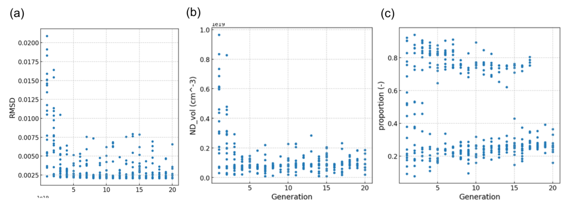
Figure 536 Evolution of (a) \(\text{RMSD}\), (b) variable $ND_vol, and (c) variable $proportion.#
The evolution of the fitness function \(\text{RMSD}\) and of optimized variables $ND_vol and $proportion is shown in Figure 536.
We minimized \(\text{RMSD}\) down to about 2 meV, with most simulation remaining below 4 meV.
The $ND_vol was found to be below 2e18 cm-3, while proportion between the doping in each barrier got established at about 0.2-0.3.
Figure 537 (a) $proportion vs $ND_vol in the last generation (b) Comparison of the evolved electronic band structure (color lines) with the target (gray lines).#
Figure 537 shows that EA-based optimization of the initially unknown parameters substantially improves the agreement between the numerically calculated spectrum and the results reported in [Novik2005].
- To practice
Perform simulations and plot the spectrum of a QW with symmetric doping in both external layers; use, e.g., ndop = [add]
Compare the spectra calculated for asymmetric and symmetric doping. Do you observe any differences? Explain your answer.