

Electronic band structure of 2DHG in silicon inversion layers under pseudomorphic strain | 1D#
Last update: 2026-04-27
- Files for the tutorial located in nextnano++\examples\electronic_band_structures
band-structure-kp_inv-layer-Si_Fischetti_2003_1D_(001).nnpband-structure-kp_inv-layer-Si_Fischetti_2003_1D_(011).nnpband-structure-kp_inv-layer-Si_Fischetti_2003_1D_(111).nnpband-structure-kp_inv-layer-Si_Fischetti_2003_1D_(001)_tensile.nnpband-structure-kp_inv-layer-Si_Fischetti_2003_1D_(001)_compressive.nnp
- Important output files
bias_00000/Quantum/probabilities_shift_quantum_region_kp6_00000.datbias_00000/Quantum/Dispersions/dispersion_quantum_region_kp6_XXXX.fld
Contents
Introduction#
This tutorial aims to reproduce the figures presented in [FischettiJAP2003] Note that the crystal growth direction is along the z axis although it becomes along x axis in nextnano++.
Unstrained silicon inversion layer with (\(001\)) surface orientation#
kpdispersion_Si_Fischetti_2003_1D_(001).nnp is used in this section.
The figures below (Figure 541) aim to reproduce Fig.1(a), and Fig.4(a) of [FischettiJAP2003].
surface_no_strain.jpg)
Figure 541 Some characteristics of the unstrained silicon inversion layer with (\(001\)) surface orientation.#
Figure 541 (a) shows the valence edges (where the heavy and light hole band edges are degenerate) and the six lowest hole wave functions of a Si inversion layer (triangular-well approximation) for \(\bf{k} = 0\) (i.e. \(k_{x} = k_{y} = 0\)) where the z axis is oriented along the [\(001\)] direction.
The potential energy of the well is given by
\[V(z') = eF_{s}z'\]
where \(F_{s}\) is the surface field. In the figure, the electric field is \(F_{s} = -1000\;\mathrm{kV/cm}\). Note that in the figure z is shifted by 1 nm: \(V(z = 1) = V(z' = 0)\). One can clearly distinguish the holes by their characters (heavy-hole-like, light-hole-like, split-off-hole-like).
The energies of the six lowest-lying hole subbands for the (\(001\)) surface of the unstrained Si inversion layer are plotted as a function of the applied electric field (i.e. as a function of the triangular-well potential) in Figure 541 (b). The subband energies are measured from the surface potential. Our results are in excellent agreement with Fischetti’s results. The symbols are calculated values, the connecting lines are added as a guide to the eye. The hole energies are taken to be positive, in contrast to the figure above (Figure 541 (a)) The labels of the curves (hh, lh, and so) are taken from Fischetti’s paper. We do not perform this analysis within nextnano++ because it is not important for quantitative results.
Figure 541 (c), (d), and (e) show the equienergy lines of the lowest lying heavy hole, light hole, and split-off hole subbands for the (\(001\)) surface of the unstrained silicon, respectively. Only one spin state is plotted for clarity. The x axis points along the [\(100\)], the y axis along the [\(010\)] direction of the crystal coordinate system.
The eigenvalues are spin-degenerate only at \(\bf{k}\) \(= (k_{x}, k_{y}) = 0\), but differ for non-zero \(\bf{k}\). The plots show the \(k_{||}\) dispersions of the lowest heavy hole (1st eigenstate, (c)), the lowest light hole (3rd eigenstate, (d)), and the lowest split-off hole (5th eigenstate, (e)).
Unstrained silicon inversion layer with (\(011\)) surface orientation#
kpdispersion_Si_Fischetti_2003_1D_(011).nnp is used in this section.
The figures below (Figure 542) aim to reproduce Fig.2(a), and Fig.4(b) of [FischettiJAP2003].
surface_no_strain.jpg)
Figure 542 Some characteristics of the unstrained silicon inversion layer with (\(011\)) surface orientation.#
Figure 542 (a) shows the valence edges (where the heavy and light hole band edges are degenerate) and the six lowest hole wave functions of a Si inversion layer (triangular-well approximation) for \(\bf{k} = 0\) (i.e. \(k_{x} = k_{y} = 0\)) where the z axis is oriented along the [\(011\)] direction. The potential energy of the well is given in the same way as in Figure 541, with a magnitude of \(-1000\;\mathrm{kV/cm}\). One can clearly distinguish the holes by their characters (heavy-hole-like, light-hole-like, split-off-hole-like).
The energies of the six lowest-lying hole subbands for the (\(011\)) surface of the unstrained Si inversion layer are plotted as a function of the applied electric field in Figure 542 (b). The subband energies are measured from the surface potential. Our results are in excellent agreement with Fischetti’s results. The plotting method is the same as in Figure 541 (b), and we also do not perform an analysis on the labels (hh, lh, and so) of each curve.
Figure 542 (c), (d), and (e) show the equienergy lines of the lowest lying heavy hole, light hole, and split-off hole subbands for the (\(011\)) surface of unstrained silicon, respectively. Only one spin state is plotted for clarity. The x axis points along the [\(100\)], the y axis along the [\(01\bar{1}\)] direction of the crystal coordinate system.
The eigenvalues are spin-degenerate only at \(\bf{k}\) \(= (k_{x}, k_{y}) = 0\), but differ for non-zero \(\bf{k}\). The plots show the \(k_{||}\) dispersions of the lowest heavy hole (1st eigenstate, (c)), the lowest light hole (5th eigenstate, (d)), and the lowest split-off hole (9th eigenstate, (e)).
Unstrained silicon inversion layer with (\(111\)) surface orientation#
kpdispersion_Si_Fischetti_2003_1D_(111).nnp is used in this section.
The figures below (Figure 543) aim to reproduce Fig.3(a), and Fig.4(c) of [FischettiJAP2003].
surface_no_strain.jpg)
Figure 543 Some characteristics of the unstrained silicon inversion layer with (\(111\)) surface orientation.#
Figure 543 (a) shows the valence edges (where the heavy and light hole band edges are degenerate) and the six lowest hole wave functions of a Si inversion layer (triangular-well approximation) for \(\bf{k} = 0\) (i.e. \(k_{x} = k_{y} = 0\)) where the z axis is oriented along the [\(111\)] direction. The potential energy of the well is given in the same way as in Figure 541, with a magnitude of \(-1000\;\mathrm{kV/cm}\).
The energies of the six lowest-lying hole subbands for the (\(111\)) surface of the unstrained Si inversion layer are plotted as a function of the applied electric field in Figure 543 (b). The subband energies are measured from the surface potential. Our results are in excellent agreement with Fischetti’s results. The plotting method is the same as in Figure 541 (b), and we also do not perform an analysis on the labels (hh, lh, and so) of each curve.
Figure 543 (c), (d), and (e) show the equienergy lines of the lowest lying heavy hole, light hole, and split-off hole subbands for the (\(111\)) surface of unstrained silicon, respectively. Only one spin state is plotted for clarity. The x axis points along the [\(11\bar{2}\)], the y axis along the [\(\bar{1}10\)] direction of the crystal coordinate system.
The eigenvalues are spin-degenerate only at \(\bf{k}\) \(= (k_{x}, k_{y}) = 0\), but differ for non-zero \(\bf{k}\). The plots show the \(k_{||}\) dispersions of the lowest heavy hole (1st eigenstate, (c)), the lowest light hole (3rd eigenstate, (d)), and the lowest split-off hole (9th eigenstate, (e)).
1% tensilely strained silicon inversion layer with (\(001\)) surface orientation#
kpdispersion_Si_Fischetti_2003_1D_(001)_tensile.nnp is used in this section.
The figures below (Figure 544) aim to reproduce Fig.5(a), and Fig.7(a) of [FischettiJAP2003].
surface_tensile_strain.jpg)
Figure 544 Some characteristics of the \(1\;\%\) tensilely strained silicon inversion layer with (\(001\)) surface orientation.#
Figure 544 (a) shows the valence edges (where the heavy and light hole band edges are no longer degenerate) and the six lowest hole wave functions of a tensilely strained Si inversion layer (triangular-well approximation) for \(\bf{k} = 0\) (i.e. \(k_{x} = k_{y} = 0\)) where the z axis is oriented along the [\(001\)] direction. The tensile in-plane strain in the \((x,y)\) plane is \(1\;\%\). The potential energy of the well is given in the same way as in Figure 541, with a magnitude of \(-1000\;\mathrm{kV/cm}\).
The energies of the six lowest-lying hole subbands for the (\(001\)) surface of the tensilely strained Si inversion layer are plotted as a function of the applied electric field in Figure 544 (b). The subband energies are measured from the surface potential which is assumed to be at \(0\;\mathrm{eV}\) for the unstrained valence band edges. After application of strain, the highest valence band edge is the light hole band edge at \(96.72\;\mathrm{meV}\). Our results are in excellent agreement with Fischetti’s results.
At low electric fields (\(-300\;\mathrm{kV/cm}\) and \(-400\;\mathrm{kV/cm}\)), the third hole eigenstate is the second light hole state (lh2), whereas for higher fields this is the split-off hole state (so1).
The plotting method is the same as in Figure 541 (b), and we also do not perform an analysis on the labels (hh, lh, and so) of each curve.
Figure 544 (c), (d), and (e) show the equienergy lines of the lowest lying heavy hole, light hole, and split-off hole subbands for the (\(001\)) surface of \(1\;\%\) tensilely strained silicon, respectively. Only one spin state is plotted for clarity. The x axis points along the [\(100\)], the y axis along the [\(010\)] direction of the crystal coordinate system.
The eigenvalues are spin-degenerate only at \(\bf{k}\) \(= (k_{x}, k_{y}) = 0\), but differ for non-zero \(\bf{k}\). The plots show the \(k_{||}\) dispersions of the lowest light hole (1st eigenstate, (d)), the lowest heavy hole (3rd eigenstate, (c)), and the lowest split-off hole (5th eigenstate, (e)).
1% compressively strained silicon inversion layer with (\(001\)) surface orientation#
kpdispersion_Si_Fischetti_2003_1D_(001)_compressive.nnp is used in this section.
The figures below (Figure 545) aim to reproduce Fig.6(a), and Fig.7(b) of [FischettiJAP2003].
surface_compressive_strain.jpg)
Figure 545 Some characteristics of the \(1\;\%\) compressively strained silicon inversion layer with (\(001\)) surface orientation.#
Figure 545 (a) shows the valence edges (where the heavy and light hole band edges are no longer degenerate) and the six lowest hole wave functions of a compressively strained Si inversion layer (triangular-well approximation) for \(\bf{k} = 0\) (i.e. \(k_{x} = k_{y} = 0\)) where the z axis is oriented along the [\(001\)] direction. The compressive in-plane strain in the \((x,y)\) plane is \(1\;\%\). The potential energy of the well is given in the same way as in Figure 541, with a magnitude of \(-1000\;\mathrm{kV/cm}\).
The energies of the six lowest-lying hole subbands for the (\(001\)) surface of the compressively strained Si inversion layer are plotted as a function of the applied electric field in Figure 545 (b). The subband energies are measured from the surface potential which is assumed to be at \(0\;\mathrm{eV}\) for the unstrained valence band edges. After application of strain, the highest valence band edge is the heavy hole band edge at \(15.47\;\mathrm{meV}\). Our results are in excellent agreement with Fischetti’s results.
Again, we have crossings of the subbands. At small confining fields, the effect of confinement is compensated by the effect of strain.
The plotting method is the same as in Figure 541 (b), and we also do not perform an analysis on the labels (hh, lh, and so) of each curve.
Figure 545 (c), (d), and (e) show the equienergy lines of the lowewst lying heavy hole, light hole, and split-off hole subbands for the (\(001\)) surface of \(1\;\%\) compressively strained silicon, respectively. Only one spin state is plotted for clarity. The x axis points along the [\(100\)], the y axis along the [\(010\)] direction of the crystal coordinate system.
The eigenvalues are spin-degenerate only at \(\bf{k}\) \(= (k_{x}, k_{y}) = 0\), but differ for non-zero \(\bf{k}\). The plots show the \(k_{||}\) dispersions of the lowest heavy hole (1st eigenstate, (c)), the lowest light hole (3rd eigenstate, (d)), and the lowest split-off hole (5th eigenstate, (e)).
Unstrained silicon inversion layer with (\(001\)) surface orientation with different \(k_{||}\) points#
kpdispersion_Si_Fischetti_2003_1D_(001).nnp is used in this section. However, the number of \(k_{||}\) points in dispersion is different from the result above.
The figure below (Figure 546) show how the number of \(k_{||}\) points affects the simulation results. The system is the same as the one we use in Figure 541, however, with different \(k_{||}\) points. The equienergy lines are plotted for \(E - E_0 = -25\;\mathrm{meV}\) where \(E_0\) is the eigenvalue of corresponding subbands at \(\bf{k}\) \(= (k_{x}, k_{y}) = 0\).
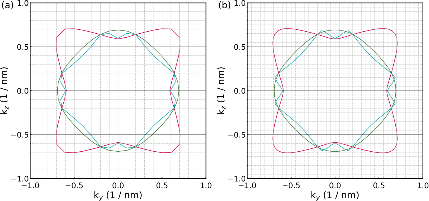
Figure 546 The dispersion for 441 \(k_{||}\) points ((a)), and for 1681 \(k_{||}\) points ((b)) for the (\(001\)) surface of the unstrained silicon under the electric field (\(F_{s} = -1000\;\mathrm{kV/cm}\)).#
The grid points on the Figure 546 correspond to the \(k_{||}\) points in the simulation. The figure shows that a smaller number of \(k_{||}\) points is sufficient to obtain accurate results in this system.