

Electronic band structure of holes in a GaN/AlGaN QW#
Last update: 2026-04-21
- Files for the tutorial located in nextnano++\examples\quantum_wells
wz_III-N_AlGaN-QW_bands_Park_JJAP_2000_1D.nnp
This simulation computes electronic band structures of electrons and holes of a 3 nm GaN QW strained to barriers made of Al0.2Ga0.8N. The system is modelled as a superlattice with thickness of the barriers set to 8.4 nm following [Park2000] with material parameters taken from both [ParkChunag2000] and [Park2000]. Poisson equation is solved first using bulk-like densities of states and taking polarization charges into account. Then Schrödinger equations is solved either using 6-band \(\mathbf{k} \cdot \mathbf{p}\) method only for valence bands (as in [Park2000]) or 8-band \(\mathbf{k} \cdot \mathbf{p}\), just for reference. Both approaches produce very similar results in the valence bands.
Note that when comparing band structures calculated using this simulation against the reference [ParkChunag2000], three major differences are visible. The first is global energy shift. It is due to that we are solving Poisson equation assuming that the Fermi level is at 0 eV. The second obvious difference is that when calculating band structure for the polar growth directions, here(0001) and (10-12), our band structures are not degenerate for the wave vectors \(k \neq 0\). Kramer’s degeneracy is lifted. It is due to that our Hamiltonian considers lack of inverse symmetry of the entire heterostructure, which is not the case in the original reference. The third difference are qualitative shapes of the lower energy bands. The source of this difference is expected to arise from the asymmetry of the system included in our Hamiltonian, actual periodicity of the system in our simulation, and unknown valence band offset used in the publication.
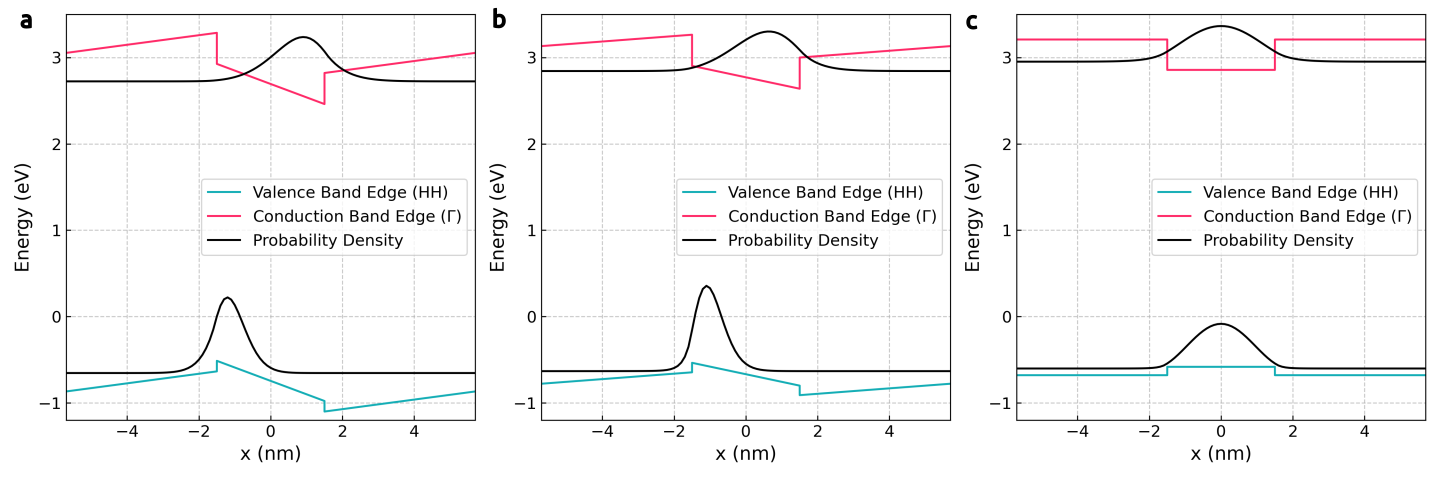
Figure 539 Energy profiles and probability densities of (a) (001)-, (b) (10-12)-, and (c) (10-10)-oriented 3 nm Al0.2Ga0.8N/GaN QW structures calculated using 6-band \(\mathbf{k} \cdot \mathbf{p}\) method for valence bands and 1-band effective mass model for the conduction band#
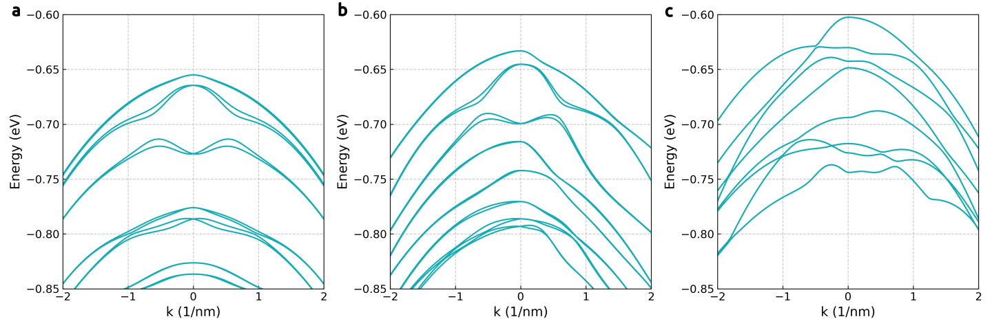
Figure 540 Valence band structures of (a) (001)-, (b) (10-12)-, and (c) (10-10)-oriented 3 nm Al0.2Ga0.8N/GaN QW structures calculated using 6-band \(\mathbf{k} \cdot \mathbf{p}\) method.#
- Acknowledgment
This site is co-funded by European Union within the project CHIPS of Europe connecting universities and industry to train the next generation of semiconductor experts.