
Efficient method for the calculation of ballistic quantum transport - The CBR method (2D example)#
Last update: 2026-04-27
- Files for the tutorial located in nextnano++\examples\transmission
transmission_CBR_Mamaluy_JAP_2003_2D.nnp
- Important output files
bias_00000/bandedges.fldbias_00000/Quantum/device/Gamma/probability_*.fldbias_00000/Quantum/lead_*/Gamma/probabilities_shift_*.datbias_00000/CBR/device/Gamma/transmission.dat
Contents
Warning
The description of the setup is invalid. Now we are importing the potential from analytical functions.
Introduction#
In this tutorial, we apply the Contact Block Reduction (CBR) method to a Aharonov-Bohm-type structure with a large barrier in the middle of the device.
This tutorial is based on [MamaluyCBR2003] and [BirnerCBR2009].
The input file Transmission_CBR_Mamaluy_JAP_2003_2D_holes.nnp simulates holes instead of electrons.
Simulation setup#
First, we look into the structure of the device. Figure 586 shows the calculated conduction band edge of the device.
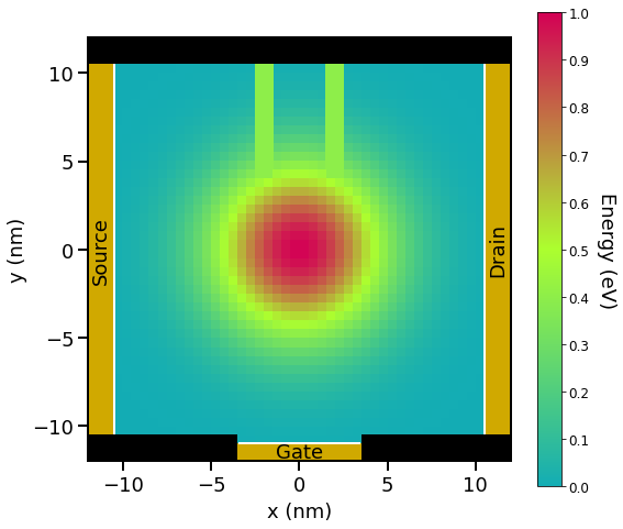
Figure 586 OUTDATED FIGURE: The calculated conduction band edge. The center of the device \(\left((x, y) = (0, 0)\;\mathrm{(nm)}\right)\) is AlAs and the energy is \(1.0\;\mathrm{(eV)}\). The vicinity of the edges of the device is GaAs and the energy is \(0\;\mathrm{(eV)}\). The double potential barrier is set so that the energy is equivalent to \(0.4\;\mathrm{(eV)}\). Note that the blacked out areas are set up with barriers of infinite height.
bias_00000/bandedges.fld#
The image below shows the 3-dimenional conduction band edge. Note that the height of the infinite potential barriers are set to \(2.0\;\mathrm{(eV)}\) for teh purpose of generating the figure.
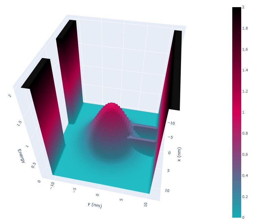
Figure 587 OUTDATED FIGURE: Potential landscape#
The device is connected to three leads called ‘source’, ‘gate’, and ‘drain’ indicated by white lines in Figure 586
In the middle of the device a Gaussian-shaped potential barrier repels the electrons from the center. The energy profile is given by
where \(E_{c,0} = 1.0\;\mathrm{(eV)}\) and \(a\;=\; 5\;\mathrm{(nm)}\), following [MamaluyCBR2003].
In the upper part of the device, a thin tunneling double barrier is present with the height \(0.4\;\mathrm{(eV)}\).
In addition, the infinite potential barriers surround the device as shown as blacked out areas in Figure 586.
This potential landscape is obtained by importing analytically defined electrostatic potential with opposite sign, see $potential_profile.
The effective electron mass is assumed to be constant throughout the device and equal to \(0.3m_{0}\).
Effectively, the simulation is set such that neumann_shifted boundary conditions are used at the leads, and Dirichlet elsewhere due to high barriers.
Note the following points.
To get results similar to shown in [MamaluyCBR2003] and [BirnerCBR2009], the dimensions of the potential elements are slightly modified relative to the reported values. This is attributed to the difference in the way boundary conditions set in nextnano++ and in original publications.
For each energy \(E\) (energy step is equal to 0.0005) where the transmission coefficient \(T(E)\) has to be calculated, a matrix of size 95 \(\mathrm{\times}\) 95 has to be inverted. The size of 95 is determined by the sum of the number of grid points in each lead that are in contact to the device.
Lead 1 (Source): 41 grid points
Lead 2 (Gate): 13 grid points
- Lead 3 (Drain): 41 grid points
in total: 95 grid points
The total CPU time for calculation of the transmission \(T(E)\) in this example is about 5 seconds for 303 eigenstates.
Note that we do not take the increase in grid points number due to the increase in the gate length into account.
Transmission#
Figure 588 shows the calculated transmission coefficients of the various lead combinations \(T_{12}\), \(T_{23}\), and \(T_{13}\). For the orange-dashed lines 100 % (1681 of 1681) of all eigenvectors were used whereas for the light-blue lines only 18 % (303 of 1681) had to be calculated. You can see that reducing the eigenvectors to 18 % or even 7 % (118 of 1681) of the total eigenvectors does not result in significant changes in \(T(E)\), especially at lower energies. This means that one does not have to calculate all eigenvalues of the device Hamiltonian which grossly reduces CPU time. A small percentage of eigenvalues suffices for \(T(E)\) in relevant energy range of interest.
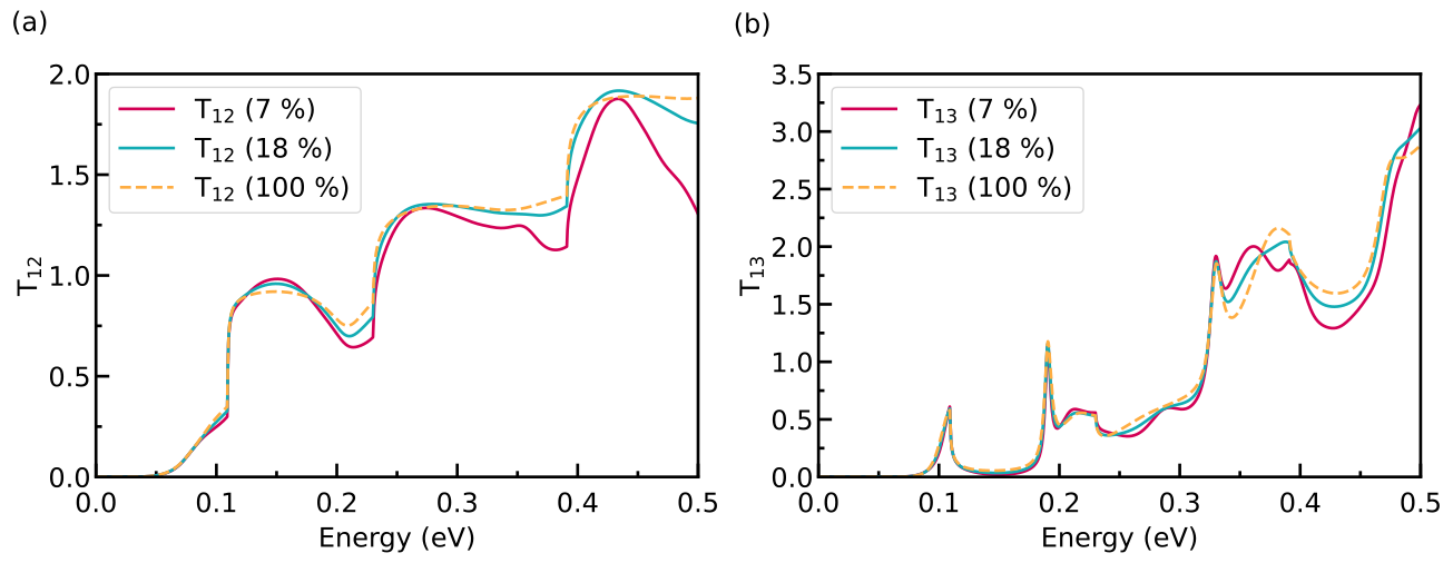
Figure 588 OUTDATED FIGURE: The transmission coefficient \(T(E)\) of a 2D sample with 3 leads. \(T_{12}\) in (a), whereas \(T_{13}\) in (b).
bias_00000/CBR/transmission_device_Gamma.dat#
The nextnano++ results differ slightly from the [MamaluyCBR2003] and [BirnerCBR2009].
- Reasons:
The potential energy profile in the device and in the leads is not identical, as well as the dimensions of the barriers.
The dimensions of the device are not identical as explained (See the attention below for further information).
Therefore, the eigenenergies and the wave functions in the device, and in the leads differ slightly which explains the small deviations.
The 16th eigenstate is a resonance state of the lower transmission path.
1st resonance: the 16th eigenstate: \(0.119\;\mathrm{(eV)}\)
The square of the 16th wave function with the conduction band is shown below. (bias_00000/Quantum/probabilities_shift_device_Gamma.fld)
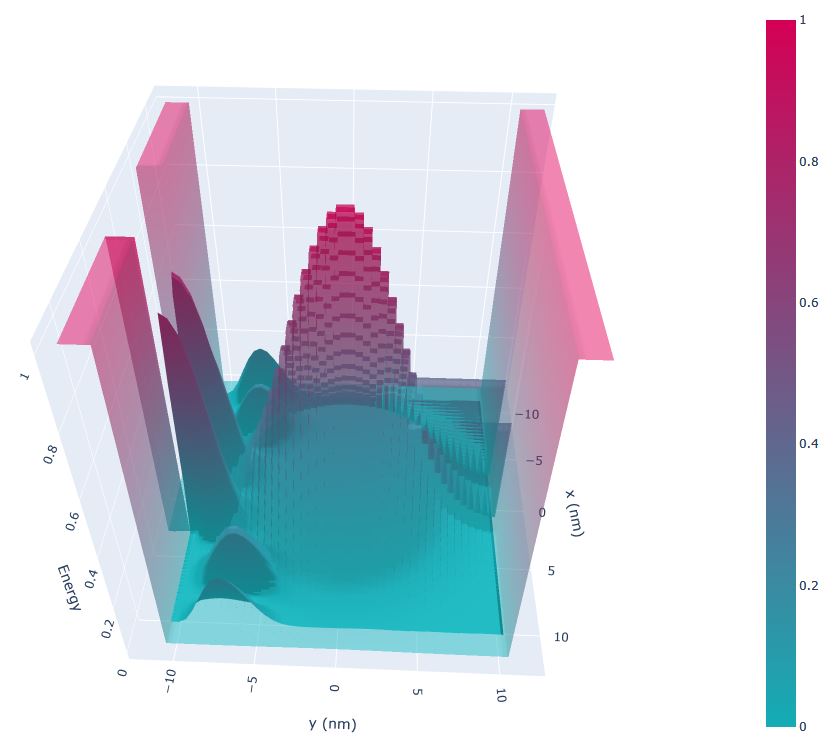
Figure 589 The 16th eigenstate#
Note that the square of the wave function is rescaled so that you can see the shape clearly.
The 26th eigenstate and 29th eigenstate are resonance states of the double barrier.
- 1st resonance:
the 26th eigenstate: \(0.177\;\mathrm{(eV)}\) (delocalized)
the 29th eigenstate: \(0.193\;\mathrm{(eV)}\) (more localized)
- 2nd resonance:
the 56th eigenstate: \(0.311\;\mathrm{(eV)}\) (delocalized)
the 59th eigenstate: \(0.328\;\mathrm{(eV)}\) (more localized)
the 61th eigenstate: \(0.336\;\mathrm{(eV)}\) (delocalized)
the 63th eigenstate: \(0.347\;\mathrm{(eV)}\) (delocalized)
the 64th eigenstate: \(0.352\;\mathrm{(eV)}\) (more localized)
TO BE CHECKED
The follow figure shows the square of the wave function of the 26th eigenstate with the conduction band. (bias_00000/Quantum/probabilities_shift_device_Gamma.fld)
You can clearly see that it is a resonance state of the double barrier and corresponds to the second peak in the light-blue transmission curve \(T_{13}\) from source to draian around \(190\;\mathrm{(meV)}\).
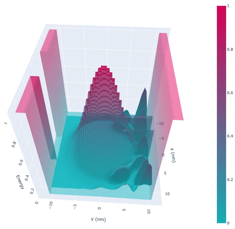
Figure 590 OUTDATED FIGURE: The 26th eigenstate#
Note that the square of the wave function is rescaled so that you can see the shape clearly.
Lead modes#
Figure 591 shows the lead modes of the gate, and the source (which is identical to the drain). In the transmission curve \(T_{12}(E) = T_{23}(E)\), the transmisson shows a step-like behavior which is related to the energies of lead 2 (‘gate’).
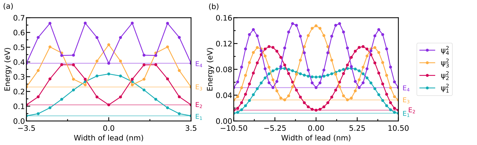
Figure 591 OUTDATED FIGURE: The lead modes of lead 2 (‘gate’) are shown in (a), whereas the lead modes of lead 1, 3 (‘source’, ‘drain’) are shown in (b).
bias_00000/Quantum/probabilities_shift_lead_X_Gamma.dat#
This tutorial also exists for nextnano³.