

Electronic band structure of tri-layer InAs/GaxIn1-xSb/InAs quantum well#
Last update: 2026-06-02
- Available for our customers upon request.
zb_III-V_GaInSb-InAs_TQW_SA_Meyer_2025_1D.nnp
- Main adjustable variables
$temperaturetemperature
$GaSb_in_central_wellpercentage of GaSb in the GaxIn1-xSb alloy
$Nc,$Nvnumber of states in conduction (electron) and valence (hole) bands (needed for the k·p model);
$Lx_barrier,$Lx_QW_outer,$Lx_QW_centralthicknesses of AlS, InAs, and GaInSb layers, respectively;
$IF_dispersioncalculating the quantum dispersion (1=”yes”, 0 = “no”).
Contents
Introduction#
Traditional TIs based on HgTe/CdTe are not ideal for practical applications, in particular due to their relatively small energy gap and the pronounced temperature dependence of both the band ordering and the TI-NI phase transition. These factors strongly limit the observation of the Quantum Spin Hall effect (QSHE) in such systems to low temperatures, typically not exceeding 15 K, and thus restrict the use of HgTe quantum wells in topological electronics. This limitation motivates the search for alternative materials.
A promising alternative is provided by TIs based on InAs/GaSb, which offer advantages such as scalability, electrical tunability, and the persistence of protected edge transport at elevated temperatures [Krishtopenko2018]. One approach to increasing the inverted band gap in InAs/GaSb-based heterostructures is to replace the GaSb layers with GaxIn1-xSb alloys and to suppress structural inversion asymmetry by introducing an additional InAs layer. Combining these two strategies, recent experiments have demonstrated the existence of the QSHE in inverted InAs/GaxIn1-xSb/InAs trilayer QWs at temperatures up to 60 K [Meyer2025].
In this tutorial, we present the energy band structure of the tri-layer TI shown in panel (a) of Figure 538. The heterostructure consisting of InAs/Ga0.68In0.32Sb/InAs is sandwiched between two AlSb NIs.
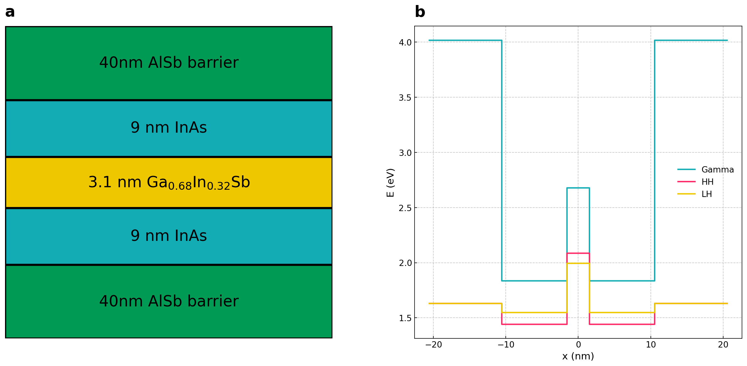
Figure 538 (a) The schematics of the tri-layer TI, which was studied in [Meyer2025] (b) Energy profiles corresponding to the schematics.#
Simulations#
We employ the 8-bands \(\mathbf{k} \cdot \mathbf{p}\) model to calculate the band edge profiles and the energy spectrum. Simulations are one-dimensional, the simulation’s axis coincides with the growth direction.
Note
This tutorial includes preliminary numerical results. Therefore, the agreement between our simulations and the results reported in [Meyer2025] is not yet optimal.
The band-edge profiles of the tri-layer QW (shown in panel (a) of Figure 538) are presented in panel (b) of:numref:zb_III-V_GaInSb-InAs_TQW_SA_Meyer_2025_1D_1. The figure compares the results reported in [Meyer2025] (grey curves) with those obtained from numerical simulations using the nextnano software (colored curves). To align the reported and simulated results, small energy offsets, which do not affect the physical properties, have been introduced.
The indirect gap in the trilayer topological insulator is determined by the energy separation between the bands E2 and E1. The 3D dispersion surfaces of these bands are shown in panel (a) of Figure 539.
[Meyer2025] reports a gap of 27 meV, while our numerical simulations yield a value of 22.5 meV. This corresponds to an acceptable deviation of approximately 4.5 meV (\(\approx\) 17%). Panel (b) of Figure 539 illustrates the energy bands E1, E2, and H2 of the trilayer quantum well shown in panel (a) of Figure 538. Grey and colored curves represent the results reported in Ref. [Meyer2025] and those obtained from our numerical simulations, respectively. The agreement between the reported and calculated energy bands is not yet optimal, but remains acceptable.
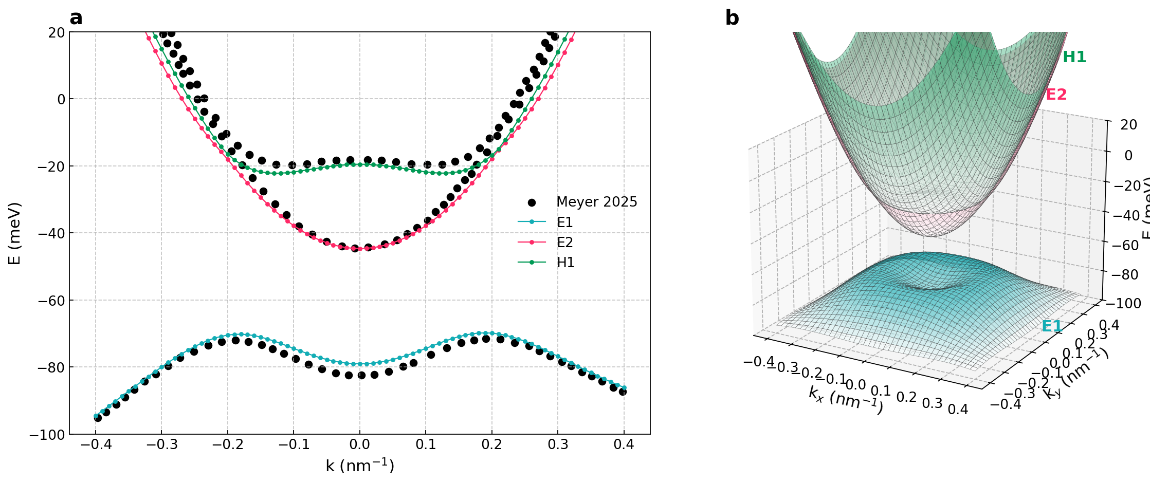
Figure 539 (a) Energy bands E1, E2, and H2 of the tri-layer QW. (b) 3D surfaces of E1 and E2 bands of the tri-layer QW. The indirect gap (\(\approx 25 \text{ meV}\)) is governed by the energy split between the bands E2 and E1.#