
Electronic band structures and phase transition in CdxHg1-xTe-based quantum well#
Last update: 2026-04-27
- Available for our customers upon request.
zb_II-VI_CdHgTe_QW_JPSJ_Koenig_2008_1D.nnpzb_II-VI_CdHgTe_QW_JPSJ_Koenig_2008_1D.py
- Main adjustable variables
$NUME,$NUMEnumber of states in conduction (electron) and valence (hole) bands (needed for the \(\mathbf{k} \cdot \mathbf{p}\) model);
$TEMPtemperature (K);
$grid_spacingstep of the space grid (nm)
$x_alloypercentage of Cd in the CdxHg1-xTe alloy
$AAA,$BBBwidth of the quantum well and barriers (nm)
$STRAINtaking into account strain (0 = “no”, 1 = “yes”)
Contents
Introduction#
In this tutorial, we focus on the energy spectrum and bulk states (i.e., states not localized at the edges) of quantum wells (QWs) based on CdxHg1-xTe. These materials were used in the first successful realization of 2D time-reversal invariant topological insulators (TI) [König2007]. The simulated device is schematically shown in Figure 531. A layer of CdxHg1-xTe, \(0 \leq x \leq 1\), is sandwiched between two CdTe barriers, which are normal insulators. The inner layer can be either topologically trivial or nontrivial, depending on the Cd concentration, \(x\), and the QW width, \(d_{QW}\).
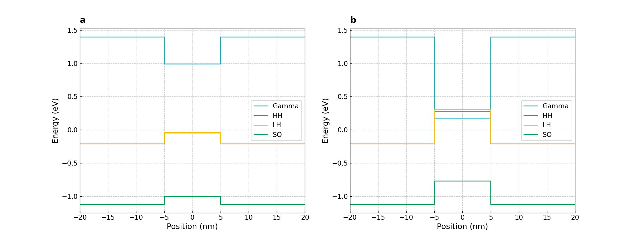
Figure 531 The energy profile of the CdTe/CdxHg1-xTe/CdTe quantum wells with (a) \(x = 0.3\) and (b) \(x = 0.05\). The width of the QW is \(d_{QW} = 10\) nm.#
Modeling confined states in CdTe/CdxHg1-xTe/CdTe QWs#
We employ the 8-bands \(\mathbf{k} \cdot \mathbf{p}\) model to calculate the band structure and the bulk states. Simulations are one-dimensional, the simulation’s axis coincides with the growth direction.
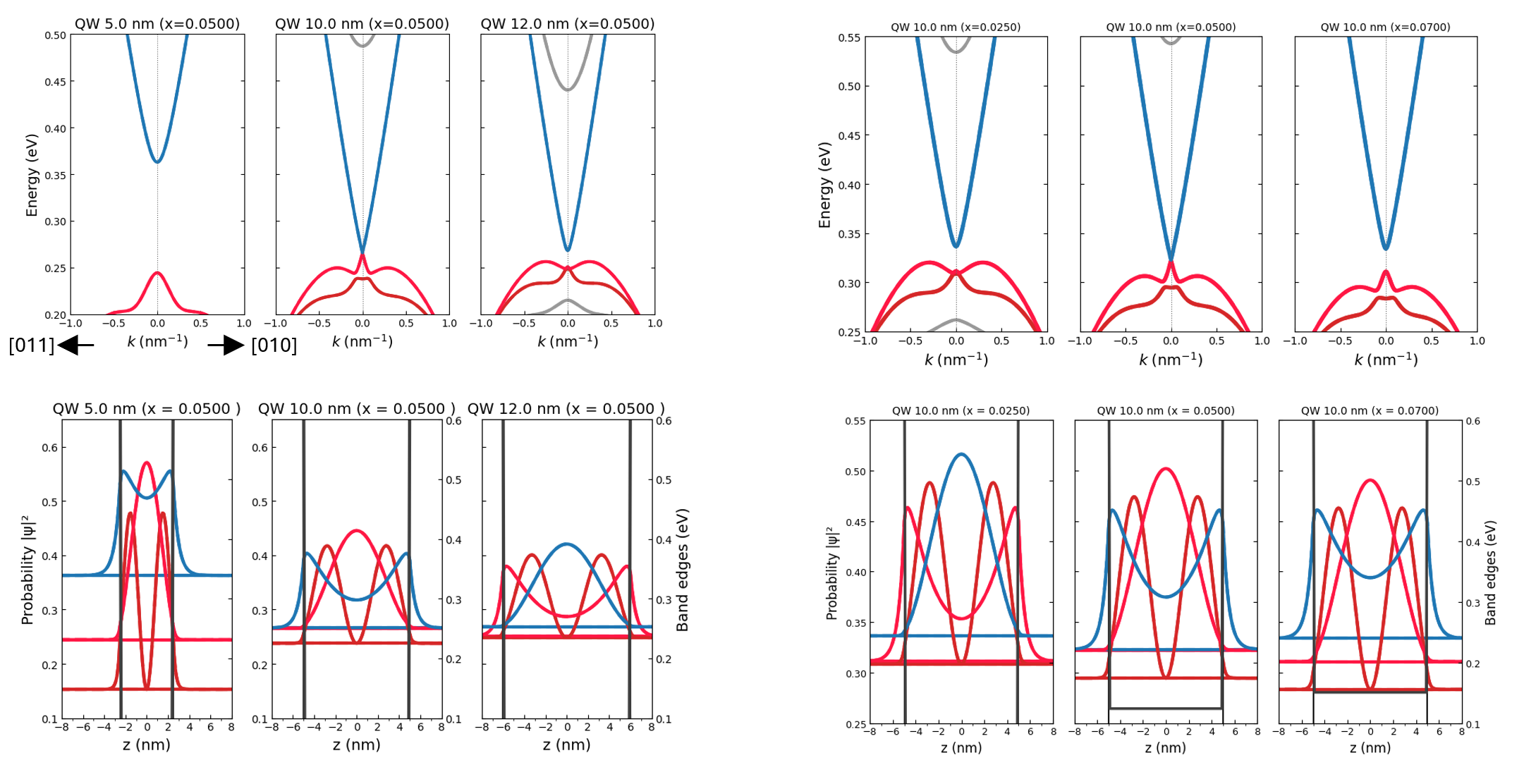
Figure 532 (a-f) Upper row: Energy spectrum of the QW with the Cd concentration \(x\) = 0.05. Blue/red lines show the empty conduction / filled valence bands, respectively. Lower row: Spatial dependence of the probability densities, obtained as the squared moduli of the corresponding states evaluated at the \(\Gamma\) -point. The QW width is: \(d_{QW} \approx 5\) nm (left column), 10 nm (central column), and 12 nm (right column). The energy profile of the CdTe/CdxHg1-xTe/CdTe QWs? (g-l) Upper row: Energy spectrum of the QW of the width \(d_{QW} \approx 10\) nm ADD k-directions. Blue/red lines show the empty conduction / filled valence bands, respectively. Lower row: Spatial dependence of the probability densities, obtained as the squared moduli of the corresponding states evaluated at the \(\Gamma\) -point. The Cd concentration is: \(x\) = 0.025 (left column), 0.05 (central column), and 0.07 (right column).#
Figure 2 shows the energy spectrum (upper row) and the probability densities (lower row) for the QWs with different widths \(d_{QW}\) and Cd concentrations \(x\). All relevant parameters are indicated in the figures and specified in the captions. The blue / red curves in the energy spectrum correspond to the empty conduction / filled valence bands, respectively. The probability densities are obtained as the squared moduli of the corresponding states evaluated at the \(\Gamma\)-point.
At \(d_{QW} \approx 10\) nm, \(x \approx 0.05\), the gap between the conduction and valence bands vanishes, signalling a transition between different phases. To investigate the nature of this transition, we analyze the spinor composition of the states at the \(\Gamma\)-point (see Figure 3). Different colors indicate contributions from the conduction band (Cb), heavy-hole bands (Hh), light-hole bands (Lh), and the spin-orbit split-off band (So), each with two spin components (1 and 2). The analysis focuses on the compositions of bands numbered [9,10] and [11,12], which are grouped in pairs due to their degeneracy. We observe that the relative contributions of the Cb and Hh components to these states interchange as the parameters pass through the critical point \(d_{QW} \approx 10\) nm, \(x \approx 0.05\). This behavior provides clear evidence of the phase transition.
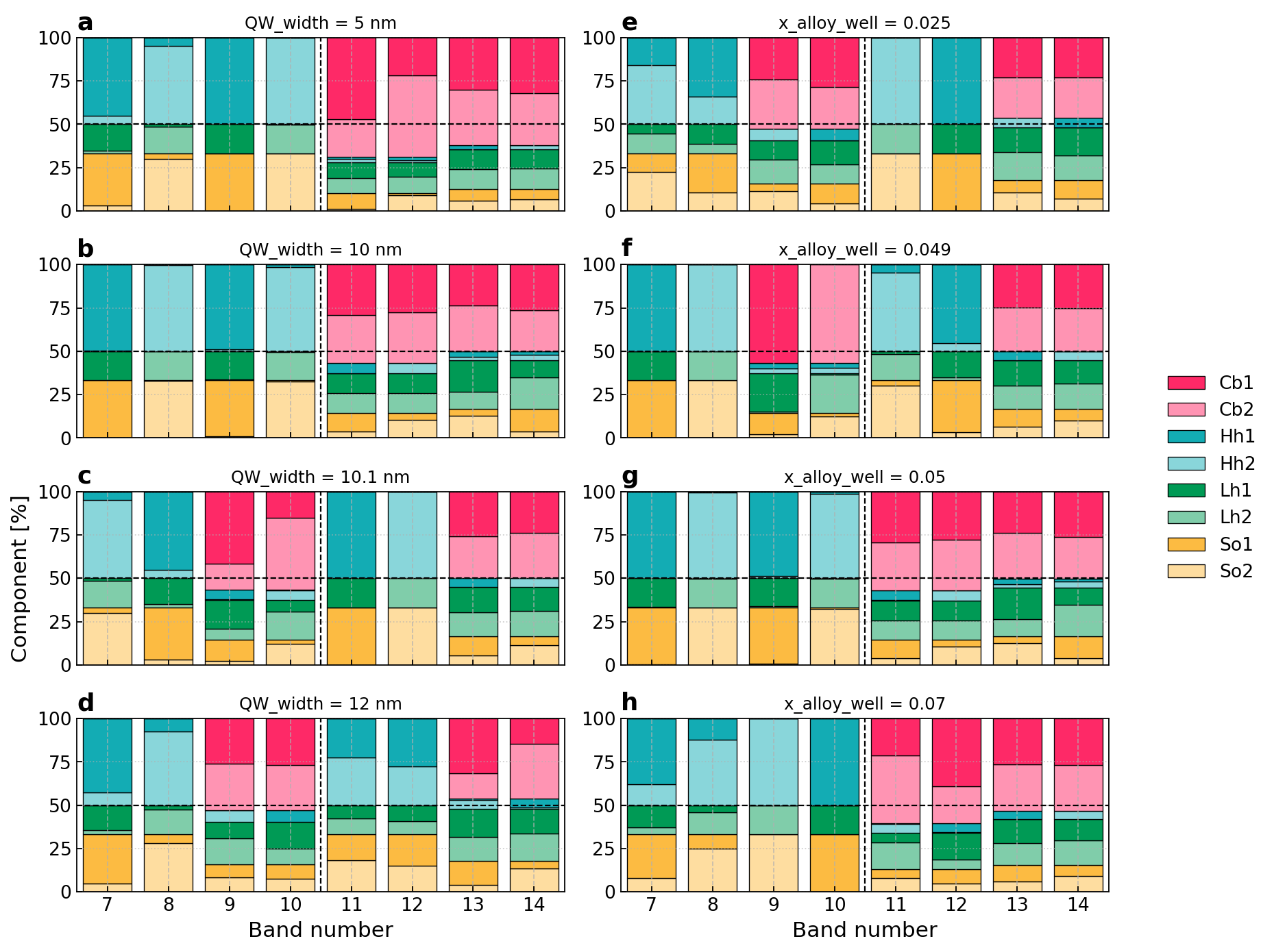
Figure 533 (a-d) Spinor compositions of states of the \(\Gamma\)-point calculated at the fixed Cd density \(x\) = 0.05 and various widths of the QW, cf. Figure 2. (e-h) Spinor compositions of states of the \(\Gamma\)-point calculated at the fixed QW widths, \(d_{QW}\) = 10 nm, and various Cd densities, cf. Figure 3#
Energy spectrum of CdxHg1-xTe/HgTe/CdxHg1-xTe QWs#
Finally, we compare the results of the numerical simulations, performed using the nextnano software, with the QW spectrum reported in [König2008]. The composition of the heterostructure used in that work is shown in Figure 4 (a).
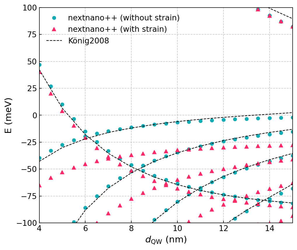
Figure 534 The energy of the states in the QW as a function of the QW width in the \(\text{Cd}_{0.3}\text{Hg}_{0.7}\text{Te}/\text{Cd}_{0.95}\text{Hg}_{0.05}\text{Te}/\text{Cd}_{0.3}\text{Hg}_{0.7}\text{Te}\) heterostructure with the well width \(d_{QW}=10\,\text{nm}\).#
To reproduce the results reported in [König2008], we used the material parameters from [add] and introduced an energy offset that does not affect the physical properties. Figure 7 shows very good agreement between the energy bands reported in the literature and those obtained from our numerical simulations.
- To practice
Perform simulations and plot the critical line (consisting of critical points) on the plane \(d_{QW}\) vs \(x\).
Explain the qualitative behavior of the critical line which you observe as \(x\) increases.