
Modeling Quantum Effects in Large Gated Systems#
Last update: 2026-07-28
Large memory consumption and long runtimes are usually the challenge when performing 3D-simulations of large devices with high accuracy. Based in our experience simulating large number of devices, we created a methodology that will assist you to set up the input files in a very efficient way. Figure 263 summarizes the three phases in the development of these files:
reduction of the dimensionality
optimization of the grid for electrostatics problems
setting up the input file for the quantum computations
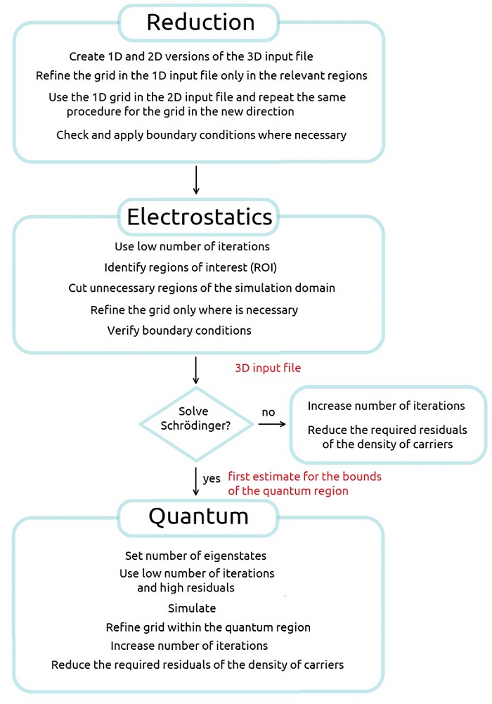
Figure 263 Methodology for 3D-simulation of large devices.#
The main idea in all steps is to define the necessary grid in the shorter time as possible.
These tutorials focus on refining grids only for selected regions where high accuracy is needed.
Reducing the dimensionality of the problem by creating 1D- and 2D- versions of the system are generally very useful to identify which regions do not require a fine grid.
Additionally, by convenient application of boundary conditions, some regions can be completely eliminated from the simulation domain.
A typical example is the substitution of substrate by an adequate boundary condition, that in nextnano++ we denominate contact.
It is important to optimize the grid always step by step: first in 1D simulations, then gradually adding more dimensions.
Even for self-consistent solution of the Schrödinger-Poisson equations we always suggest to set up the input file solving only the Poisson equation, even when not accurate enough. These solutions can be very useful for identifying unnecessary regions to be eliminated from the simulation domain, and to refine the grid only where is actually necessary.
Our focus will be the evolution of the residuals at the beginning of the convergence process. Then, as we mentioned above, it is not expected to obtain accurate results, but only the trends of these residuals.
If no quantum computations are required this would be the point to reduce the residuals in the convergence process for obtaining the results with the accuracy desired.
Similarly, as done in the two previous steps, the definition of the quantum region can be the secret to the final tuning of the 3D-input file. Starting with the results of the electrostatic problem we can identify the regions of interest for such simulations where the grid has to be refined. The identification of a suitable number of eigenvalues for the self-consistent simulations is a crucial procedure that must be performed. It is also important to be aware of the boundary conditions that are adequate at the bounds of the quantum region.
We can take advantage of the one symmetry that the device can present for making a first exploration of these issues. This will save you memory and time.
Each of these procedures are explained in details and with a practical example in three independent tutorials containing guidelines concerning how to simulate large devices in three dimensions efficiently.
Reducing dimensionality of large 3D designs#
- Files for the tutorial located in nextnano++\examples\numerics
large-3D-systems-reduction_1D.nnplarge-3D-systems-reduction_2D.nnplarge-3D-systems-reduction_3D.nnp
- Relevant keywords
- Important output files
/bias_00000/bandedges.dat/bias_00000/bandedges_1d_xz_Si_2DEG.datlarge-3D-systems-reduction_2D_nnp.log
Introduction#
Accurate simulations depend on finding a compromise between a very fine grid, the memory consumption and the corresponding runtime. Nevertheless tuning the grid resolution for 3D simulations of large devices can become highly time expensive, when a methodological approach is missing.
The purpose of this tutorial is to provide some suggestions with the aim of reducing the time for choosing a suitable grid and of its impact on the solutions. It is the first part of the methodology that we strongly recommend being followed.
In this first step we will show what we can learn from simulations in 1D and 2D of the device, for building a suitable grid when modeling the most important regions on it.
To make it very practical, we will introduce in the next section a structure that can be used in a semiconductor-based quantum computer as an example. The quantum operations are performed by handling the bias of gates on the top of the device, that controls the transport of the carriers through the active region. This is a typical device where all transport of carriers is electrostatically dominated. For this reason, a consistent simulation of the charge distribution and the potential in the device is imperative to reach accuracy enough to identify the most important modes of operation at each position.
Most of these devices can present hundreds of nanometers than represent a heavily time-consuming procedure when performing 3D simulations. The suggestions presented below will assist you to define the grid that can reduce the bottlenecks of larger simulations. There is not a unique way to do it, but it has been used for numerous cases, not only for quantum computing, and provided very good results in most of them.
Device to be simulated#
Figure 264 presents a simplified version of a device that consists basically of a 7 nm-Si layer buried in a silicon dioxide structure [Kriekouki2022]. This silicon layer will be used as the channel where electrons can transit through.
Gates ( FGS, FGD, LG1, LG2, LG3 ) are deposited at few nanometers of top of the interface of the Si channel with the surrounding oxide gates. By applying specific combinations of biases to these gates it is possible to change the electrostatic potential and, in this way, to control the states present in the structure for each configuration. The source and drain contacts can be seen as the reservoirs that will provide the carriers that will propagate in the channel.
Additionally, applying bias to a back gate under the thick layer of oxide under the Si-channel can allow or prevent the transport through the device.
The dimensions of this device to be simulated is the order of 400 nm x 800 nm x 70 nm. The last dimension ( 70 nm ) does not include the back gate and substrate regions that, as we will see soon, can be removed from the simulation domain. Nevertheless, the relevant results in the active regions are very localized and can require grid resolutions of order of few nanometers or smaller.
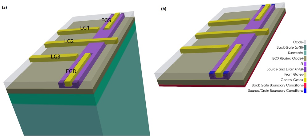
Figure 264 Device to be simulated. The Si-channel is buried in the oxide. FGS, FGD, LG1, LG2, and LG3 are used to shape the electrostatic potential.The back gate is used to allow or to interrupt the transport of electrons through the channel. The source and drain are the reservoirs of carriers.#
Reducing the dimensionality of the problem#
Before setting up input files for 3D simulations we recommend to start with 1D or 2D computations. Even when quantum computations are necessary, use only semiclassical models ( Poisson ), just enough to identify the most relevant aspects of the transport in some critical regions.
You can either start designing the 3D version and reduce it to the 1D and 2D versions, or to develop first the 1D version and expand it to the final 3D structure.
For making the design more flexible, use variables to represent the most important coordinates of the structure. Name the variables according its 3D representation in the device reference frame, in contrast to the simulation reference frame. The simulation system is defined in the global{ } section of the input file. Figure 265 presents the most important coordinates in the device coordinate system, used in all versions of the input files of our example.
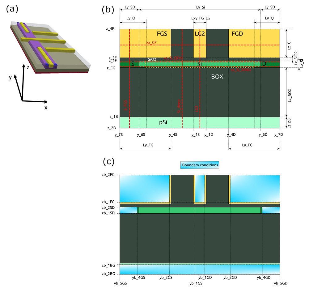
Figure 265 Device reference system and most important coordinates used for 1D and 2D simulations: (a) the 3D representation, (b) structure definition, and (c) structure after applying boundary conditions to the contacts and gates. Dotted lines ( in red ) represent sections defined in the input files.#
Here is an example how to perform the modification from 3D to 2D input file. Suppose that one region is defined in the 3D input file by:
cuboid{
     x = [$x_3F, $x_3L]
     y = [$y_4GS, $y_4GD]
     z = [$z_EG, $z_2F]   # growth direction in the simulation reference system for 3D simulations
}
where the growth direction is along the z-axis ( vertical ) in the device coordinate system.
This has to be translated to a 2D-input file as:
rectangle{
     x = [$y_4GS, $y_4GD]
     y = [$z_EG, $z_2F]   # growth direction in the simulation reference system for 2D simulations
}
and to a 1D-input file as:
line{
     x = [$z_EG, $z_2F]   # growth direction in the simulation reference system for 1D simulations
}
Avoid renaming variables when changing from one dimension to another.
Why this is important?
In nextnano++ the growth direction is aligned to different axis, depending on the dimensionality of the simulation. For 1D simulations, the x-axis of the simulation system is the growth direction. Nevertheless, when we change to the 2D version, the code interprets that the y-axis as the growth direction. Finally, 3D simulations assumes ( implicitly ) that the growth direction is aligned to the z-axis of the simulation system.
In the general case, the crystal orientation in the simulation system shall be changed every time we make a change of dimensionality, in the global{ } section of the input file. This shall be also be taking into account concerning the strain{ } section of the input file, when strain calculations are necessary ( that in this not the case in this example ).
Then, reducing or expanding the input files to another dimensions will require changes in the next sections of the input file:
in global{ }: simulate1D{ }, simulate2D{ }, simulate3D{ }, and changing the crystal orientation ( when necessary )
in quantum{ } (when present): boundary{ }
in strain{ } (when present): growth_direction
in structure{ }: line{}, rectangle{}, cuboid{} or another shapes
in contacts{ }
Last but not least, also regions that must not appear in the plane ( for 2D ) or line ( for 1D ) of the simulations must be eliminated from the section`structure{ }`, quantum{ } and contacts{ }.
As example, large-3D-systems-reduction_1D.nnp and large-3D-systems-reduction_2D.nnp are input files for 1D and 2D simulations of the same device respectively.
We recommend comparing these two versions with the corresponding 3D version.
Learning from 1D Simulations#
The most frequent simplification that can be made when modeling the device is the substitution of extensive regions at the bottom of the structure, mainly the substrate and back contacts, or even buffer layers. For this device this procedure is adequate, because of the wide buried oxide layer that separates the back gate and the Si channel, our main area of interest. Figure 266 illustrates the final device to be simulated where the substrate and the back gate ( green in Figure 264 ) were substituted by boundary conditions at the bottom of the structure ( red ). This is the equivalent to set this last layer as a point or plane of reference for the electrical potential or the Fermi level to a certain value.
Additionally, gates and vias that connect the external environment with the source and drain regions can be substituted by convenient boundary conditions. We will skeep this discussion concerning how to set boundary conditions that can be explored in another tutorials of our documentation related to this very important topic. What is important to mention is that 2D or even 1D versions can become valuable for modeling the eliminated regions through use of suitable boundary conditions.
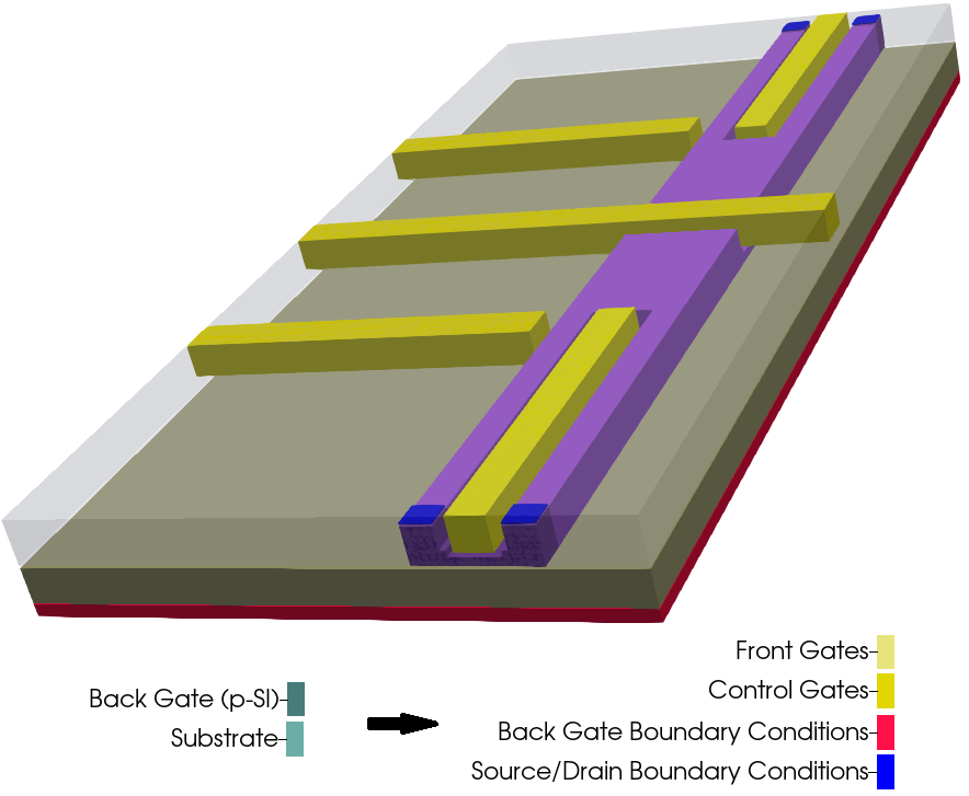
Figure 266 Regions substituted by adequate boundary conditions and final device representation#
In 1D simulations it is required to choose the direction to be simulated that depends on the geometry of the specific device. In our example, the structure consists basically of a stack of layers where the Si layer is embedded, and is biased at the top and at the bottom. Then, a natural choice for 1D simulations of devices with this characteristic is along the growth direction that, by convention in nextnano++, is aligned in this case to the x-axis of the simulation system, as discussed before.
Depending on the complexity of the device it may be required to choose different points for the 1D simulations. Figure 267 illustrates some of these points that could be explored for the device of our example. From a quick analysis of our example we can observe that the line A is the most relevant for the first tuning of the grid, because it contains the most important coordinates of the interfaces to be examined.
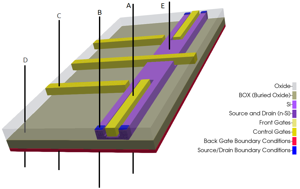
Figure 267 Representation of possible regions of study for 1D simulation in the growth direction.#
The input file large-3D-systems-reduction_1D.nnp presents the device as a stack of layers passing through one of the gates over the Si channel (line A).
This can be used to set up and/or verify the parameters used to model each material of the structure.
After simulation, we can easily identify, for example, the conduction band across this direction as shown in Figure 268.
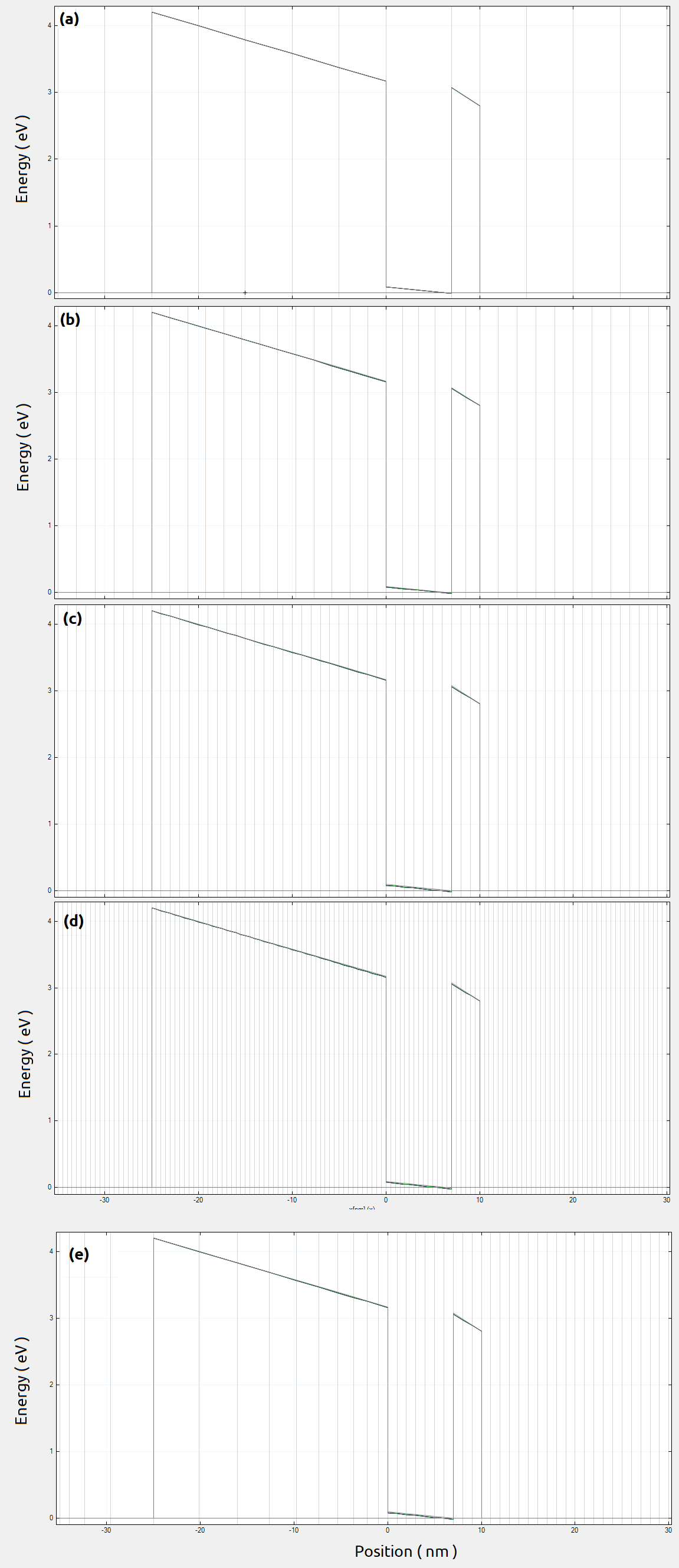
Figure 268 Conduction band resulting from 1D simulations in the growth direction along the line A for homogeneous grid resolution: (a) 5 nm, (b) 2 nm, (c) 1 nm and (d) 0.5 nm. The gray vertical lines represent the grid lines used in this simulation. (e) corresponds to a grid resolution of 1 nm inside the active region and 5 nm in the remaining parts of the structure ( in the growth direction ).#
These plots were obtained by running this input file for different homogeneous grid line spacings in the growth direction ( from a to d ). We can easily identify the most important regions: the back-gate, the buried oxide, the channel ( surrounded by oxide ) and some of the top gates. Here, the most important region is the Si-channel ( the active region ), whose grid resolution can be increased.
Such input file runs very quickly, and it is a very good starting point for choosing a suitable grid resolution. From these plots we can observe that the conduction band is not too sensitive to the choice of the grid resolution in this direction. An ideal situation is to define a finer grid spacing in the active region and a coarse grid for the remaining parts of the device. It is recommended to make the final refining of the growth direction only in the last steps of the 2D or 3D grid tuning, for saving more runtime. In our example for the next simulations it will be used 1 nm and 5 nm grid as fine and coarse grid spacing for the growth direction, respectively ( plot e in Figure 268 ).
Hint
Visualize the grid lines selecting Simulation grid in nextnanomat menu.
Refining grid in 2D Simulations#
Now it is time to perform the 2D simulations, using our input file large-3D-systems-reduction_2D.nnp.
It represents a slice of the device passing through the center of both front gates ( FGS and FGD ), parallel to the growth direction and the propagation direction, as shown in Figure 269.
This kind of representation can be very useful for defining the more convenient boundary conditions at equilibrium conditions for the gates and for the contacts. The device of our example requires these gates be modeled as highly-doped quasi-metallic regions at low temperatures. How to set them properly we invite you to visit our tutorial about contacts{ }.
At this point we will freeze the grid resolution in the growth direction, and will refine the grid spacing along the propagation direction. In this way, when talking about grid resolution or spacing we will be referring to the propagation direction.
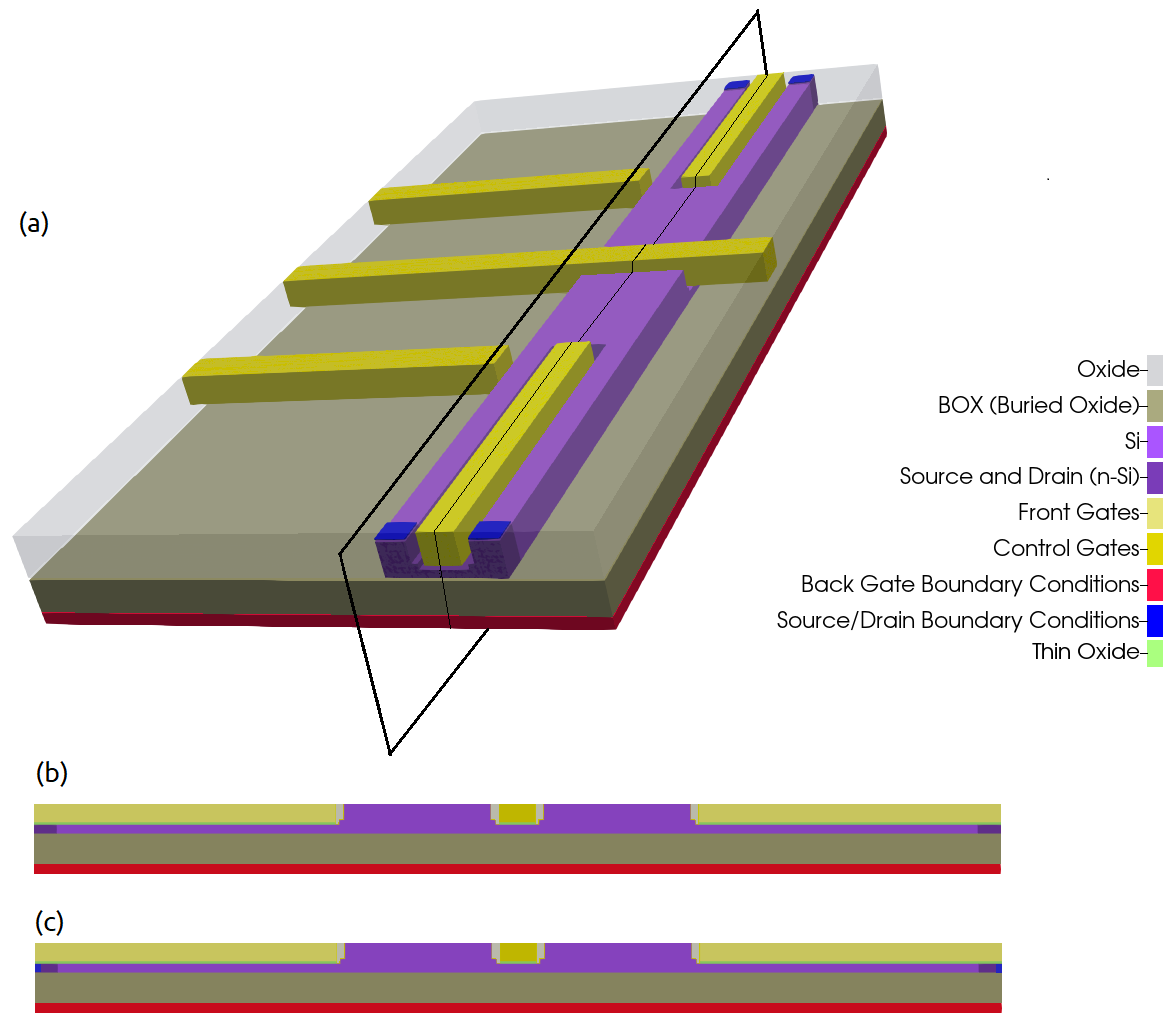
Figure 269 Slice simulated in our example.#
Our main goal of these 2D simulations is the identification of the most important regions where the grid must be refined in the propagation direction. We will focus
in the conduction band computed with different grid resolutions, that are presented in Figure 270.
The data is stored in /bias_00000/bandedges.dat of the output folder.
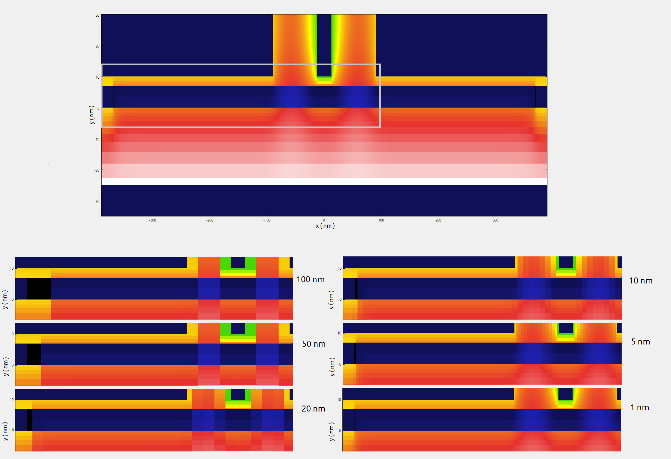
Figure 270 Conduction band along a plane containing the growth direction and the center of the front gates. This result was obtaining grounding all gates and contacts, except the front gates that were biased at 0.8 V. The upper image corresponds to the full simulation domain simulated. The region inside the gray rectangle is presented below for different grid resolutions.#
As soon we decrease the grid line spacing it becomes difficult to distinguish the results from the 2D plots. For this reason, it is recommended to include in the input file some 1D sections for both directions, that makes easier to compare the results. You will find several of these sections defined in the 2D input file of our example.
Hint
It is highly recommended to include the coordinates of all interfaces and the one used for specifying output sections and slices in the grid definition on your input file this avoids unnecessary interpolation of the results.
Figure 271 presents the comparison of the conduction band just 1 nm above the interface between the buried oxide and the Si-channel ( section xz_Si_2DEG of Figure 265 ) from 2D simulations with the different grid spacing.
The corresponding results can be found in the output files /bias_00000/bandedges_1d_xz_Si_2DEG.dat. From the image we identify that the central region from -150 and 150 nm at the most relevant for controlling the transit of carriers from one side to the other of the channel.
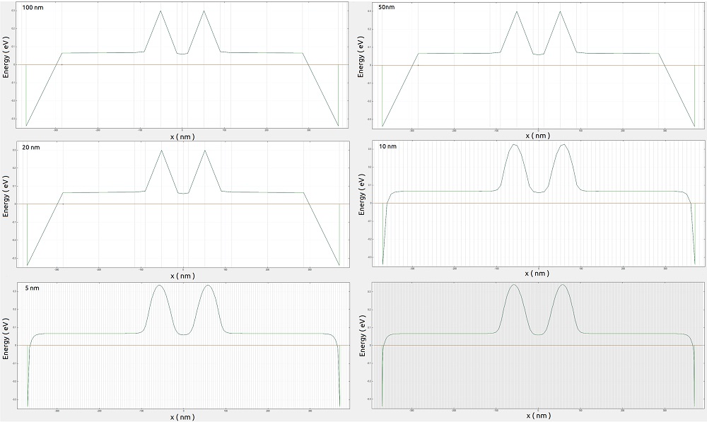
Figure 271 Conduction band at 1 nm above the interface between the buried oxide and the Si-channel ( section xz_Si_2DEG of Figure 265 ) from 2D simulations with the different grid spacing.
The gray lines correspond to the grid lines.#
In Figure 272 we can observe in detail these regions for resolutions of 1, 5, 10 and 20 nm. The central region presents similar results using fine grids, while at the borders of the simulation region, a good model of the potential requires resolutions higher than 20 nm.
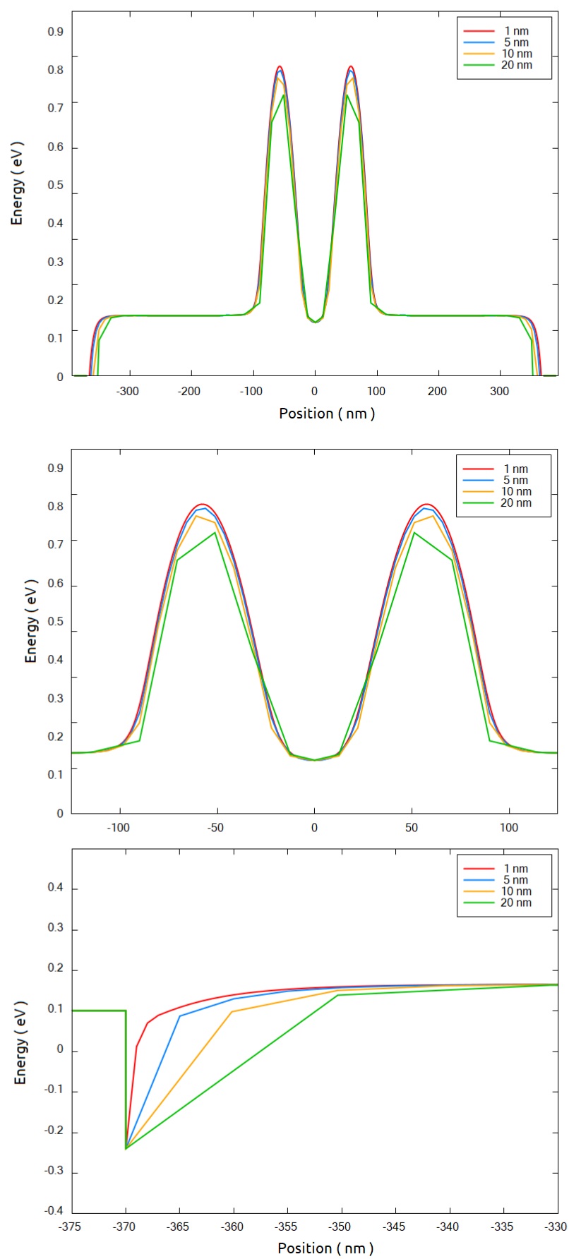
Figure 272 Comparison of the conduction band at a 1 nm above the interface between the buried oxide and the Si-channel ( section xz_Si_2DEG of Figure 265 ) from 2D simulations. The central region and the source contact regions are also shown with more details.#
The first temptation is to use the minimum resolution as possible ( 1 nm ), but this is not necessary and not recommended: we have not started the 3D simulations yet. Figure 273 shows how the simulation time scales with the number of nodes and the grid resolution. We observe that for coarse grid ( grid line spacing around 20 and 100 nm ) the time for simulation does not change too much. Nevertheless, as soon it becomes fine the time starts to increase dramatically.
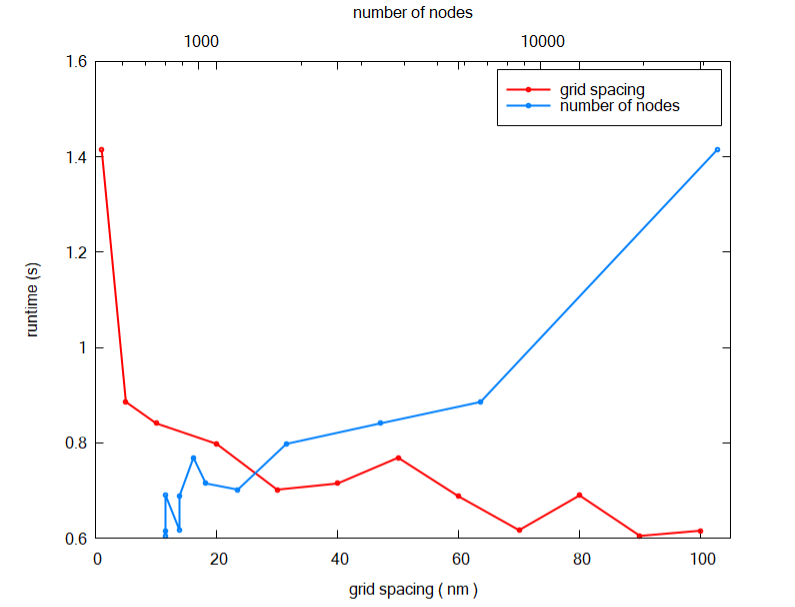
Figure 273 Runtime for 2D simulations as function of the number of nodes in the grid and the grid spacing.#
A good strategy is to define different grid spacings in the x direction: small for the relevant regions ( central and the contact ) and larger for the ones that does not change ( the remaining ).
Last but not least, this simulation was performed for a specific combination of biases to the gates ( 0.8 V to the front gates, and 0 to the other gates and contacts ). It is not necessary to simulate all bias combinations, but it is useful to check some of them that can result in larger modifications of the potential at least in active region.
- Exercise:
Run the input file
large-3D-systems-reduction_2D.nnpfor several grid resolutions and obtain the plot of Figure 273 for your system. All information required for this exercise ( number of nodes and runtime ) you can find in the filelarge-3D-systems-reduction_2D_nnp.login the output folder of each simulation.
Hint
The performance of the simulations can be improved setting the number of threads for a single simulation in the menu Tools > Options > Simulation of nextnanomat.
It is also recommended to set the tab Tools > Options > Executable the command
-b <number the cores of your system>
as additional parameter passed to the executable (field Command line of this menu). For example, if you are a user of a 6- cores-processor, write
-b 6.
Using the grid defined in the growth and propagation directions, we can expand to the third dimension.
Optimizing electrostatics simulation for large 3D designs#
- Files for the tutorial located in nextnano++\examples\numerics
large-3D-systems-poisson_2D.nnplarge-3D-systems-poisson_3D.nnplarge-3D-systems-poisson_3D_reduced.nnp
- Important output files
/bias_00000/bandedges_1d_xz_Si_QDs.dat/bias_00000/bandedges_1d_yz_Si_QDs.dat/bias_00000/density_electron_1d_xz_Si_QDs.dat/bias_00000/density_electron_1d_yz_Si_QDs.dat
Introduction#
For structures that strain computations are not needed, obtaining the electrostatic potential is the first step even when more complex computations are required.
Nevertheless, self-consistent computations of the landscape potential with the charge distribution for large devices demanding high accuracy generally consume a huge amount of memory and long execution time.
This tutorial is the second part of a methodology for reducing the time in the development of the input files for modeling such 3D structures. In this methodology we suggest to start by tuning the grid of the simulation using 2D versions of the correspondent 3D input file. Although it is not mandatory following this first step for implementing the suggestions in this tutorial, we strongly recommend its reading at Reducing dimensionality of large 3D designs, for understanding of the main concepts also used here.
We will take as an example a structure that can be used in a semiconductor-based quantum computer, that we introduced in the first tutorial of the methodology and quickly summarized below.
Device to be simulated#
Figure 274 presents a simplified version of a device found in the literature [Kriekouki2022] that consists basically of a 7 nm-Si layer buried in a silicon dioxide structure. This silicon layer corresponds to the channel where the quantum operations are performed.
The transport of the carriers depends on the combination of the voltage applied to the gates (FGS, FGD, LG1, LG2, LG3) at the top of the structure isolated from the silicon channel by a thin layer of oxide. At the bottom of the structure, just below the thick buried oxide layer, a back gate plays also an important role in the definition of the landscape potential. The source and drain contacts in this scenario act as the reservoirs that will provide the carriers that will propagate in the channel.
Applying adequate boundary conditions, the device to be simulated can be simplified as shown in the Figure 274 (shown in (b)).
Figure 274 Device to be simulated. The Si-channel is buried in the oxide. FGS, FGD, LG1, LG2, and LG3 at the top of the structure and the back-gate, between the thick oxide layer under of Si layer (BOX) and the substrate, are gates used to shape the electrostatic potential. Source and drain act as reservoirs of carriers propagating through the channel. Device (a) before and (b) after applying adequate boundary conditions.#
Starting simulations in the semiclassical domain#
The first thing we have to keep in mind is the goal of our simulation: which equations have to be solved, the accuracy we want to achieve, and other post-processing tasks that will be necessary. In our practical example is expected that under certain bias combinations a quantum dot is formed in the channel close to the lateral gates LG1 and/or LG3. Then, an accurate electrostatic potential self-consistently solved with the Schrödinger equation is required for obtaining a good estimate of the wave functions in the device, that will also be used in coherent transport calculations.
Nevertheless, self-consistent quantum computations with Poisson equation means that we need to a sufficient number of eigenvalues enough to reproduce the carrier densities that will be used in the next Poisson iterations. For this reason, the runtime of the whole simulation does not only scale with the number of nodes of the structure for the electrostatic potential calculations, but also depends on the size of the quantum region and the number of eigenvalues that has to be solved.
Then, as a general rule, setting the grid for 3D simulations is more efficient when started with semiclassical calculations, where only the Poisson equation, or even the coupled current-Poisson equations, is solved. Additionally, nextnano++ always uses the resulting potential as a first estimate for the next steps of the quantum computation and other calculations. As a rule of thumb, run and verify the results step by step. In other words, perform the next step of the computations when the previous step (the electrostatic problem) properly converged. In this tutorial we will focus only in the solution of the Poisson equation self-consistent with the semiclassical densities of electrons, for refining the grid of 3D input files. Hints for optimizing the performance of quantum simulations will be provided in a separated tutorial (Optimizing Schrödinger-Poisson self-consistent solver for electrostatic quantum dots).
Refining the grid of 3D-input files#
It is more efficient following the first step of our methodology, where the grid is progressively refined in the growth and in the propagation directions, that results in the file large-3D-systems-poisson_2D.nnp for 2D simulations.
Then, it follows that the 3D version of this input file is simply the extension of the refined 2D version, that now includes the lateral gates LG1 and LG3 in the structure.
The growth direction for 3D simulations is aligned to the z-axis of the simulation domain (see file
large-3D-systems-poisson_3D.nnp).
Figure 275 shows the nomenclature of the most important points in the device coordinate system, sections and boundary conditions used in this input file.
It is clear that the previous grid tuning in 1D or 2D simulations is not a mandatory procedure: simultaneous tuning of the three axes in the 3D input file could be also performed. The disadvantage of this approach is that the execution time of each simulation depends on the number of nodes on the grid, that it is in higher number for the 3D case.
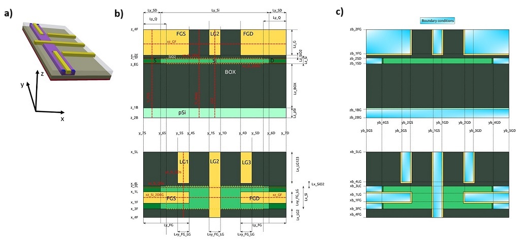
Figure 275 Device reference system and most important coordinates: (a) the 3D representation, (b) structure definition, and (c) structure after applying boundary conditions to the contacts and gates. Dotted lines (in red) represent sections defined in the input files.#
Now it is time to start the simulations. Refining of the grid in the last dimension (x-axis) does not require, initially, high accuracy. In this way, the criteria that define the end of the convergence process (residuals, for example) can be “relaxed” in these first estimates. The idea is to identify regions of interest (ROI) where a fine grid has to be necessary to a suitable description of the density of electrons or holes in the simulated domain.
This is an iterative process where, looking at the conduction bands or the density of carriers in the ROI, we will try to refine the x-grid that the resulting density presents a smooth decay. For this task, it is recommended to define 1D slices in the most important ROIs and to overlay different plots in the same image within our graphical interface (nextnanomat). In our practical example, our objective it to capture the results in the region where the quantum dots are expected to be formed and different points where the density of carriers or the potential will be analyzed. Slices where the potential presents the steepest slopes are also important to be included in this analysis.
Figure 276 shows the conduction bands of two important ROIs, for a particular combination of biases (0.8V to both front gates, 4 V at LG1 and LG3, 1.7 V at the central gate (LG2) and 0 V for the remaining gates and contacts).
In the image, the xz_Si_QDs section corresponds to a slice at the region on Si-channel close to the interface with the gate LG1 (for x = 35 nm) and 1 nm above its interface with the buried oxide (BOX), where the quantum dot is expected to be formed. xz_Si_2DEG is the slice of the conduction band along the y direction at 1 nm below the oxide under the front gates (x = 0 nm).
Also important to observe is the slice yz_Si_QDs defined by the intersection of the plane along the longitudinal axis of the LG1 gate and the plane passing at 1 nm above the interface between the Si-channel and the BOX. These sections are shown in Figure 274 using dotted lines (in red).
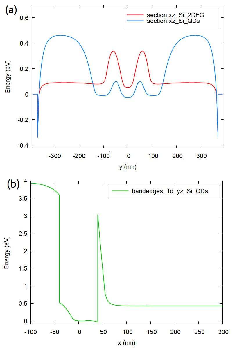
Figure 276 Slices of the conduction band in the two most relevant regions of interest for a particular combination of bias applied to the gates (see text):
(a) xz_Si_QDs, at 1 nm above the interface between the Si-channel and the BOX, close to the lateral gate LG1 (x = 35 nm), and xz_Si_2DEG, at 1 nm below the oxide under one of the front
gates (x = 0 nm), (b) yz_Si_QDs, at 1 nm above the interface between the Si-channel and the BOX, in the plane containing the longitudinal axis of the gate LG1.#
The first step of the grid definition in the third axis consists in the elimination of unnecessary areas of the device. We need to distinguish two situations: solutions of quantum mechanics problems, or solutions of the electrostatics of the device only.
The first situation, when the semiclassical computations will be followed by computation of the wave functions, will demand more attention when eliminating or even reducing areas from the simulation domain. In this case we recommend that the final size of the device be defined only when the first quantum simulations be performed. A reduction of several undesired nodes at this moment still will bring benefits, but it is important a future evaluation of the impact of these cuts in the boundary conditions for the quantum calculations. Keep in mind that the wave functions can penetrate certain interfaces. Then preserve certain margin around the interfaces in order to allow a priori that some tail of the wave function can be properly calculated.
For the other situation, when we are only interested in the electrostatic solutions, this is the appropriate moment to cut these regions from the simulation domain.
Our particular example is in the first situation, and the elimination of some unnecessary areas can be valuable. We can expect a priori that the potential of the lateral gates LG1 and LG3 close to the Si-channel does not depend on the length of these gates, because of the large potential barrier between the Si-channel and the surrounding oxide of each gate, that practically results in vanishing of the wave functions at the interface of both materials. Then, this simplifies a lot our 3D simulations, because the lateral gates can be reduced and substituted by the convenient boundary conditions.
Figure 277 presents the impact of the changes of the lateral gate lengths on the results of the conduction band for the section xz_Si_QDs.
The results are practically equal, if the gate lengths are larger than 100 nm.
Then, we will use 100 nm as the length of the lateral gates for the reduced version of the 3D input file.
This value is also reasonable when we analyze the results for the section yz_Si_QDs (the growth direction), that practically independent of the choice of the level of this reduction.
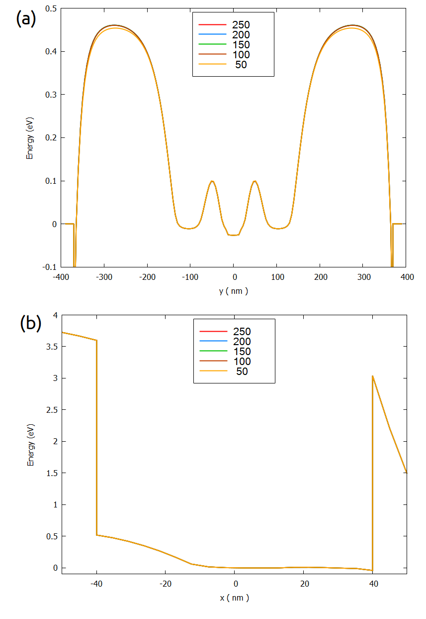
Figure 277 Conduction band in the quantum dot region as function of the length of the gates LG1 and LG3 in the simulation:
(a) slice xz_Si_QDs, and (b) slice yz_Si_QDs#
Another natural candidate to be eliminated is the region from the start of the simulation system ($x_min = $x_4F).
Figure 278 shows the results of the conduction band for different values of $x_min, for the same slices of the previous image.
In this case, the extension of the negative axis of the simulation domain plays an important role in the definition of the electrostatic potential at the left border of the Si-channel (at x = -40 nm), while the region close to the lateral gates practically does not change (at x = 40 nm).
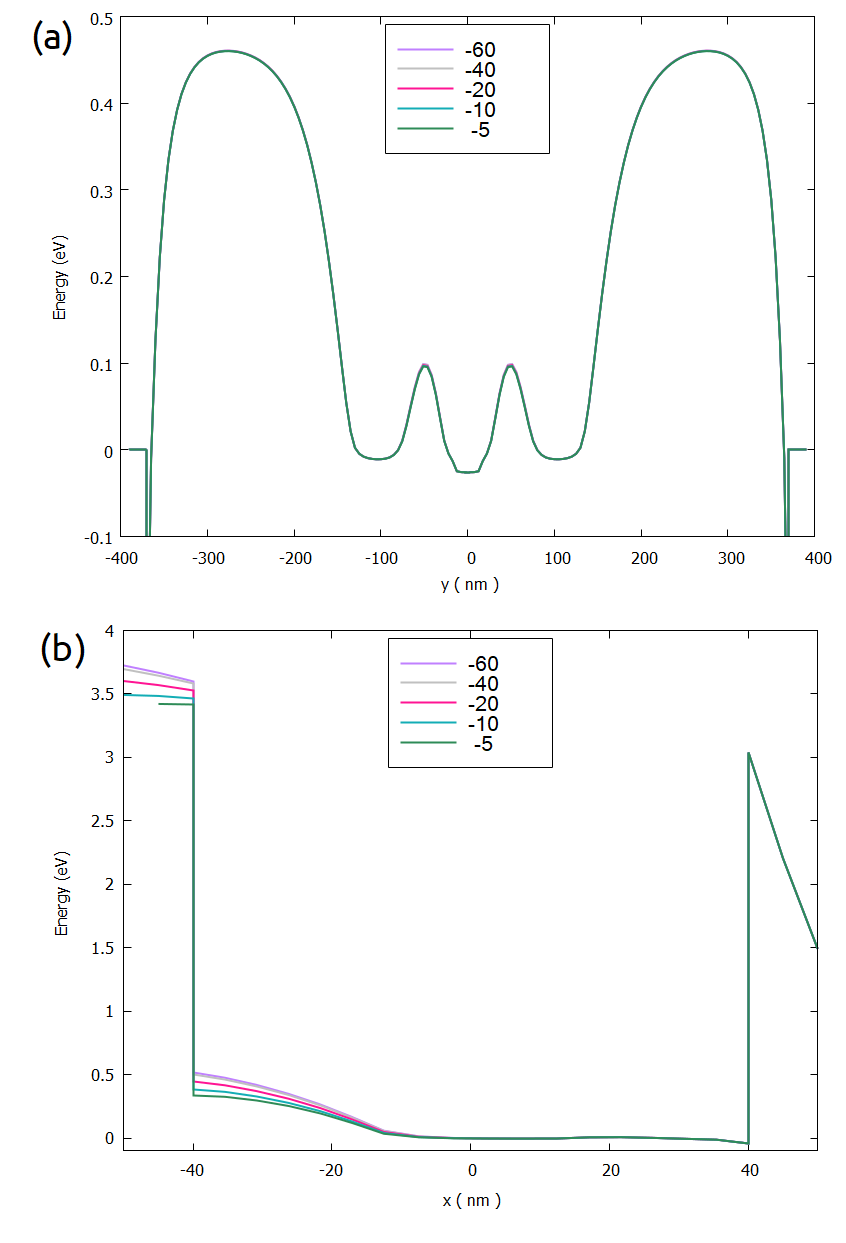
Figure 278 Conduction band in the quantum dot region as function of the value of $xmin:
(a) slice xz_Si_QDs, and (b) slice yz_Si_QDs.#
Looking at to the conduction band results not enough to decide what it is an optimal value for $xmin to be used in the next simulations.
When this happens, more careful evaluation of the impact of these cuts have to be done.
Our suggestion is to verify the goals of the simulations and to combine results.
In our example, we can overlap to the conduction bands the corresponding density of electrons (our goal) and observe the differences using different cuts in the ROIs, as illustrated in the Figure 279.
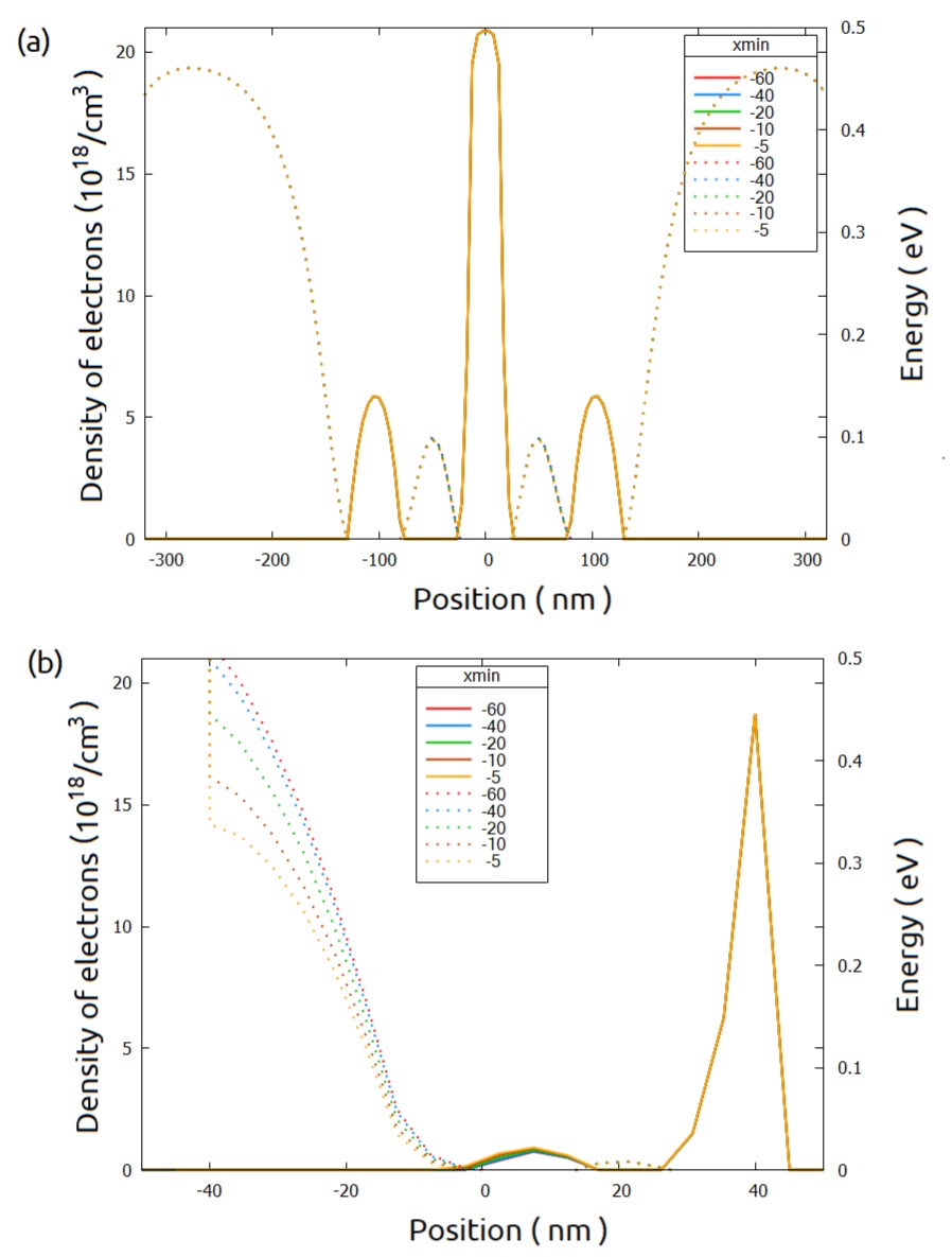
Figure 279 Conduction band (dotted lines) and density of electrons (solid lines) in the xz_Si_QDs and yz_Si_QDs.#
From this figure we can observe that in terms of electron density, they are not affected by the value of $x_min chosen. Similar analysis must be performed for all relevant results of the calculations.
large-3D-systems-poisson_3D_reduced.nnp is the resulting input file after these reductions, and it will be used in the next computations.
As we can observe, we are using a very conservative approach concerning the cuts around the Si-channel and the lateral gates, in order to give an example that would be done in a more general way.
If no quantum computations are necessary, this would be the moment of increasing the accuracy of the simulations by requiring lower residuals for the density and fermi levels, until the results (for example, density of electrons) does not change within a certain precision from one simulation to the other. If necessary, you can include some more lines in the positions of the grid for getting better results.
Once the grid is completely defined, make a final check concerning the sensitivity of the calculations with changes in the grid resolution.
Considerations if quantum computations will be required#
Semi-classical computations of the density of electrons are very useful to identify how wide is actually the region where the carriers can be observed. Specially for self-consistent calculations, this evaluation is tremendously valuable because allows us to estimate the minimum size of the quantum domain to be simulated. It is always relevant to keep in mind that the total execution time in this case will also be affected by the number of the nodes in the quantum region and the number of eigenvalues to be used for self-consistent calculations, as we mentioned before. We will discuss in the more detail in our next tutorial of the presented methodology.
From Figure 279 we could identify the bounds of the region where most of the electrons are present. Then it is natural to choose them as first good estimate for the quantum region. Nevertheless, we must not forget that this result was obtained for one a specific combination of biases applied to the gates and the contacts. Then, it is convenient to make a quick check for some other combinations in order to verify if this region need to be extended.
Figure 280 shows the density of electrons overlapped with the respective conduction band for another bias combinations. Starting from the one presented above (0.8V to both front gates, 4 V at LG1 and LG3, 1.7 V at the central gate (LG2)), we changed either the bias on the back gate, in the central gate (LG2), or simultaneously in the other lateral gates (LG1 and LG3).
We can observe that applying bias to the back gate greater than 1.0 V, will require an extension of the quantum region from [-150, 150] to [-200, 200] in the y-direction.
Changes in the bias of the lateral gates does not change too much the semi-classical density of electrons distribution.
Then, in the next step we suggest to start defining the quantum region limited to the smaller interval ([-150, 150]), at least for the first setup of the input file including quantum calculations.
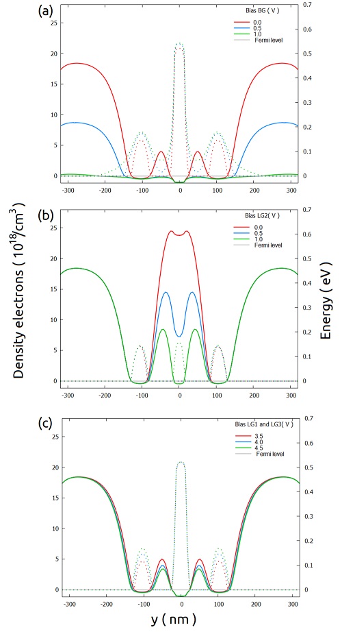
Figure 280 Conduction band (solid lines) and density of electrons (dotted lines) in the xz_Si_QDs sections changing only one of the bias of the combination discussed above:
(a) the back gate, (b) the central lateral gate (LG2), and (c) simultaneously to the lateral gates LG1 and LG3.
Here the full length of the lateral gate LG2 (250 nm) was used.#
Optimizing Schrödinger-Poisson self-consistent solver for electrostatic quantum dots#
- Files for the tutorial located in nextnano++\examples\numerics
large-3D-systems-schroedinger_3D_initial.nnplarge-3D-systems-schroedinger_3D_final.nnp
- Relevant keywords
- Important output files
/bias_00000/bandedges_1d_xz_Si_QDs.dat/bias_00000/bandedges_1d_yz_Si_QDs.dat/bias_00000/iteration_quantum_poisson.dat/bias_00000/quantum/probabilities_shift_QuantumRegion_Delta3_1d_xz_Si_2DEG.dat/bias_00000/quantum/probabilities_shift_QuantumRegion_Delta3_1d_yz_Si_2DEG.dat/bias_00000/quantum/occupation_QuantumRegion_Delta1.dat/bias_00000/quantum/occupation_QuantumRegion_Delta2.dat/bias_00000/quantum/occupation_QuantumRegion_Delta3.datnn_Large_Devices_3D_initial_version_quantum_nnp.log
Introduction#
Setting up input files for 3D-simulations of the self-consistent Schrödinger-Poisson or self-consistent Schrödinger-current-Poisson system of equations can demand some effort in terms of memory allocation and time consumption, if a systematic approach is missing. This development can become a real challenge when the dimensions of the devices are large (some can be of order of microns) and a fine grid (few nanometers) is required.
This tutorial aims to assist you to reduce such effort, and it is the third part of the methodology, that we strongly recommend being followed.
The input file large-3D-systems-schroedinger_3D_initial.nnp was obtained in the first two steps of this methodology for the structure that we will very briefly summarize in the next section.
This file presents a suitable grid resolution (only sufficient, but not optimally, refined) for obtaining a first estimate of the bounds of the region where the quantum computations will be performed.
Unnecessary regions on the devices were eliminated or replaced by convenient boundary conditions.
Following these previous steps are not mandatory for the discussion in the tutorial, but it is very advantageous avoiding grid refinement or performing such tasks directly on 3D-simulations. We remark that there is not a unique way to do it, but it has been used for numerous cases, and provided very good results in most of them.
Device to be simulated#
Figure 281 presents a simplified version of a device that is proposed as a possible semiconductor-based implementation of a quantum computer found in the literature [Kriekouki2022] with dimensions of 400 nm x 800 nm x 70 nm. It consists basically of a 7 nm-Si layer buried in a silicon dioxide layer. By applying bias to the gates deposited at the top of the structure (FTS, FTD, LG1, LG2, and LG3) and at the bottom of the oxide (the back gate) the electrostatic potential can be modified, in order to control the transport of carriers through the silicon layer (the channel of the system). The source and drain are the reservoirs of carriers.
Applying adequate boundary conditions, the simulation domain can be reduced as shown in the Figure 281 (shown in (b)). The nomenclature of the most important coordinates and sections defined in the input file are summarized in the same image in (c).
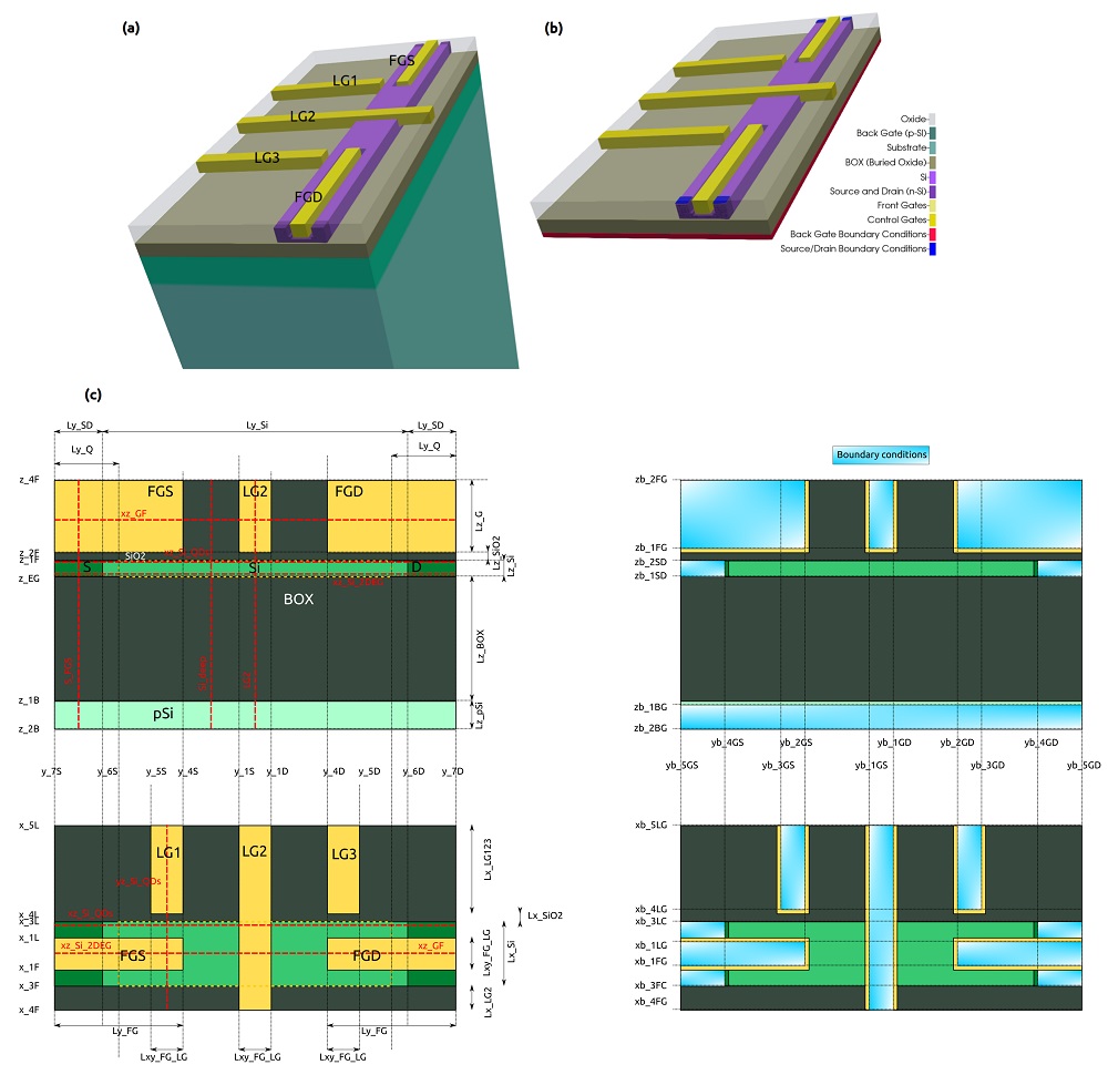
Figure 281 Device to be simulated. The Si-channel is buried in the oxide. The electrostatic potential is shaped by applying bias to the gates (FTS, FTD, LG1, LG2,LG3 and the back-gate). Source and drain act as reservoirs of carriers propagating through the channel. Device (a) before and (b) after applying adequate boundary conditions. The most important coordinates and sections (dotted lines in red) are shown in (c).#
Setting input files for self-consistent calculations of Schrödinger-Poisson equations#
As we mentioned before, self-consistent solution of Schrödinger and Poisson equations demands a good strategy in order to reduce the simulation time when tuning the grid. Usually smooth wave functions in some region of interest (ROI) require a fine grid resolution and enough number of states to compute the quantum mechanical density of carriers that iteratively will also be used in the solution of the Poisson equation.
Another important issue that show be addressed is the choice of the boundary conditions at the borders of the quantum region. It has to be constantly observed if they are consistent with the models used in the simulation.
Below we present some hints that may be explored for designing an efficient input file for 3D simulations.
Define the goals of the quantum computations#
The simulation time of self-consistent Schrödinger-Poisson simulations depends on the time expended in the solution of the Poisson equation and the time for obtaining the quantum solution.
As we showed in previous tutorials, the time for solving the Poisson equation scales with the number of nodes in the grid of the simulation domain. On the other hand, the solution of the Schrödinger equation demands runtimes scaling with the number of nodes in the quantum region, the number of eigenvalues to be computed and also the model and corresponding solver to be used.
Below we will provide some tricks related to these aspects for getting excellent results with less effort.
Optimizing the grid within the quantum regions#
1. Defining the bounds of the quantum region: at the beginning does not need to be perfect!#
The nodes in the quantum region consist on a subset of the grid points of the simulation domain that are within and at the borders of are region where the Schrödinger equation will be solved. In other words, limiting the size of the quantum region of interest (QROI) and its corresponding grid resolution in the first phase of the quantum simulations will boost the input file development.
Any previous understanding of the physical phenomena in the device may be used to introduce simplifications in the QROI design. Let us present one simplification from our practical example. A quantum dot in the Si channel is expected to be present just in the channel, close to one or both lateral gates (LG1 and LG3) depending on the bias applied to these and the other gates. In this way, if our goal is to compute the density of carriers in the region where the quantum dots appear, the number of nodes of the QROI will represent a very small subset compared with the number of nodes in the whole domain.
A trick for estimating the bounds of the quantum region is to look at the density of electrons from the semi-classical calculations (solving only the Poisson equation).
Please, refer to our tutorial Optimizing electrostatics simulation for large 3D designs concerning some considerations that may be taken into account.
Figure 282 presents the results of such simulations for the conduction band overlapped with the semi-classical density of electrons for the sections xz_Si_QDs and yz_Si_QDs under a particular combination of biases (0.8V to both front gates, 4 V at LG1 and G3, 1.7 V at the central gate (LG2) and the remaining gates and contacts are grounded).
These sections, shown with red dotted lines in Figure 282, correspond to slices at the region on Si-channel where the quantum dot is expected to be formed.
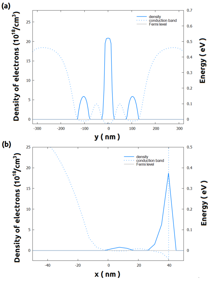
Figure 282 Conduction band (dotted lines) and semi-classical density of electrons (solid lines) in the slices xz_Si_QDs and yz_Si_QDs (see red dotted lines in Figure 282), when 0.8 V is applied to both front gates, 4 V to LG1 and LG3 and 1.7 V to the central gate LG2. The remaining gates and contacts are kept grounded.#
Although the electrostatic potential is shaped by each specific combination of bias applied to the gates, the bounds of the QROI estimated by the semi-classical electron distribution does not change too much if the biases are around the first operation point, as we showed in the tutorial concerning the electrostatic calculations mentioned above.
The bounds of the QROI resulting from this analysis are x = [-40, 40], y = [-150, 150] and z = [0, 7].
The device of our example presents a geometrical symmetry related to the plane y = 0. We can take advantage of this property by reducing even more the QROI for the first tuning of the parameters concerning quantum computations. Our main objective here is not even to get good results, but to have a first idea about the convergence process of the system of equations, the required grid resolution within the quantum region, and to verify if the boundary conditions at the borders are satisfied.
In this way we can weak a little the criteria of the convergence of the quantum_poisson solver, requiring a low number of iterations (for example 10 iterations, or $quantum_iterations = 10).
Keeping these requirements in mind we can start defining a reduced QROI with y = -150 and y = -50 as the bounds in the y-direction.
Hint
You can save some time and storage disabling all outputs files that are not relevant or did not change from one run to the other, like contacts, intrinsic density, and material.
2. Finding a suitable number of eigenvalues#
The Hamiltonian to be solved in the Schrödinger equation is specified in the section quantum{ } of the input file. In the section region{ } of our documentation you will find the models currently implemented in nextnano++. Independent of your choice we recommend to use at this point the computationally lighter one: the single-band. The relevant bands to be taken into account in these calculations must be defined in the input file. In our example, the band gap of silicon, the material of the region of interest, is defined by the minimum of the Delta band.
As we mentioned above, we need to choose a number of eigenvalues enough to compute the density of carriers from the wavefunctions obtained after each quantum iteration. This quantity will be injected in the Poisson equation in the next iteration, and a new electrostatic potential will be computed. Then, here we need to do a trade-off: the number of states can not be too small, but also not too large.
Low number of computed states generates truncated quantum density that, when included in the next iteration of the solver of Poisson equation, may change the electrostatic potential in another direction, and more frequently may not converge. On other hand larger number of states will require more computational effort unnecessary for this first tuning.
How to choose a suitable number of eigenvalues? The answer is simple: guess, compare and improve.
Remember: our grid is still coarse.
Then, this is the best moment to explore a first guess.
We recommend that, starting with 10 states, for example, to increase this number and compare some relevant results iteratively, instead of simply sweeping the variable $N_states in our input file.
Now it is time to perform the first calculations. Remember: what it is important to observe here is how the residuals behave during the convergence process when new states are added. Figure 283 shows the evolution of the residual of the density of electrons as function of the number of eigenvalues. We can see that the residual decay faster when more states are included in the computation. The resulting conduction band in two relevant sections does not change substantially for number of states larger than 20. The reason for this can be inferred from the occupation number for one of the Delta bands: it is required computing at least 20 states in order to converge that 4 states are actually occupied.
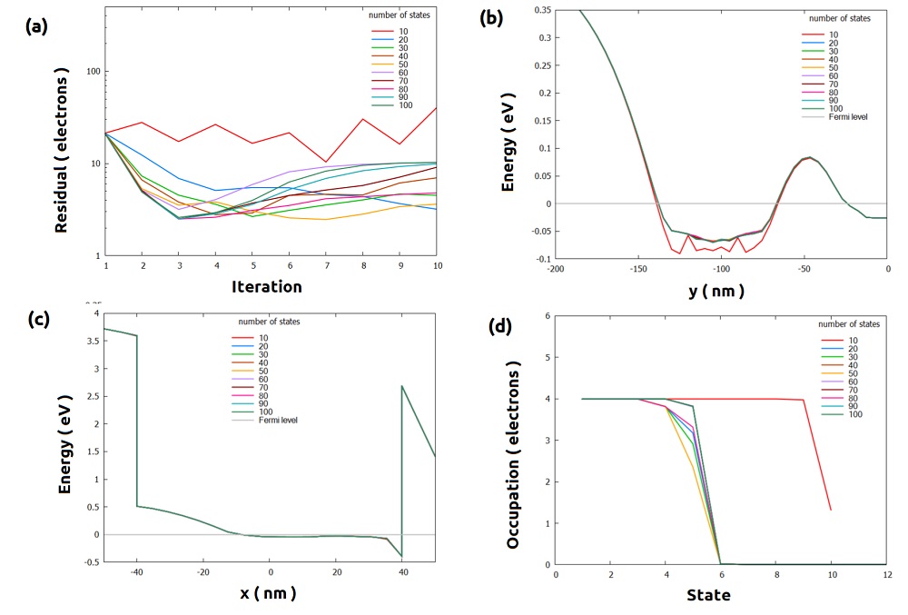
Figure 283 Results of the self-consistent Schrödinger-Poisson simulations, in the reduced QROI as function of the number of eigenstates computed, after 10 iterations. (a) The evolution of the residuals, (b) and (c) the conduction band for the sections xz_Si_QDs and yz_Si_QDs, respectively, and (d) the occupation number after only 10 iterations. These are intermediate results: the convergence process was still not completed.#
Please, be aware: we still are not getting the solutions of the system (look at the log files in the output folder, large-3D-systems-schroedinger_3D_initial.log).
The system is still coarse, and probably we are still very far from the minimum residuals to be reached, for stopping the process.
Nevertheless, this behavior of the residuals tells us that we are in the right direction.
3. Making the grid fine in the quantum region#
Let us take a look at the wavefunctions in the computations using 20 eigenstates ($N_states = 20) shown in Figure 284 for the same sections of Figure 283.
It is more convenient to use the results of the output file /bias_00000/quantum/probabilities_shift_QuantumRegion_Delta3_1d_xz_Si_2DEG.dat or /bias_00000/quantum/probabilities_shift_QuantumRegion_Delta3_1d_xz_Si_2DEG.dat that represent the values of the density probabilities in a section, shifted by the correspondent eigenvalue.
From this reason, from this point to the end of this tutorial “wavefunction” actually means shifted probability density.
The first observation is that the boundary conditions for the quantum conditions looks being suitable for the band edges in this region.
Nevertheless, the grid resolution in the x- and y-directions is actually too coarse, as expected.
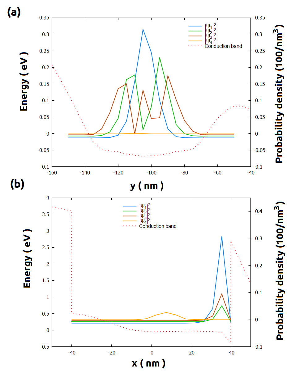
Figure 284 Wavefunctions overlapped to the conduction band from self-consistent quantum-Poisson simulations for the sections (a) xz_Si_QDs and (b) yz_Si_QDs.
The “quantum” density of electrons were computed considering 20 states and a grid resolution of 5 nm in the y-direction.
These are intermediate results: the convergence process was stopped after 10 iterations.#
To avoid explosion of the number of nodes to be simulated, we suggest modifying the grid definition by introducing new variables for the control of the grid space only within the quantum region. Including the bounds of the quantum region in the grid is also highly recommended. In our example, our previous definition of the grid in x- and y-direction:
388    xgrid{
389        line{ pos = $x_4F spacing = $space_x_4F }
390        line{ pos = $x_3F spacing = $space_x_Si }
391        line{ pos = $x_1F spacing = $space_x_Si }
392
393        line{ pos = $x_1L spacing = $space_x_Si }
394        line{ pos = $x_3L spacing = $space_x_Si }
395        line{ pos = $x_4L spacing = $space_x_4L }
396        line{ pos = $x_5L spacing = $space_x_5L }
397    }
398
399    ygrid{
400        line{ pos = $y_7S spacing = $space_y_SD }
401        line{ pos = $y_6S spacing = $space_y_SD }
402        line{ pos = $y_5S spacing = $space_y_LG }
403        line{ pos = $y_4S spacing = $space_y_LG }
404        line{ pos = $y_1S spacing = $space_y_LG }
405        line{ pos = $y_1D spacing = $space_y_LG }
406        line{ pos = $y_4D spacing = $space_y_LG }
407        line{ pos = $y_5D spacing = $space_y_LG }
408        line{ pos = $y_6D spacing = $space_y_SD }
409        line{ pos = $y_7D spacing = $space_y_SD }
410    }
will be changed to
388    xgrid{
389        line{ pos = $x_4F spacing = $space_x_4F }
390        line{ pos = $x_3F spacing = $space_x_Si }           # bound of the quantum region
391        line{ pos = $x_1F spacing = $space_x_QR }
392
393        line{ pos = $x_1L spacing = $space_x_QR }
394        line{ pos = $x_3L spacing = $space_x_QR }           # bound of the quantum region
395        line{ pos = $x_4L spacing = $space_x_4L }
396        line{ pos = $x_5L spacing = $space_x_5L }
397    }
398
399    ygrid{
400        line{ pos = $y_7S spacing = $space_y_SD }
401        line{ pos = $y_6S spacing = $space_y_SD }
402
403        line{ pos = $yq_min spacing = $space_y_QR }           # bound of the quantum region
404        line{ pos = $y_5S   spacing = $space_y_QR }
405        line{ pos = $y_4S   spacing = $space_y_QR }
406        line{ pos = $y_1S   spacing = $space_y_QR }
407        line{ pos = $y_1D   spacing = $space_y_QR }
408        line{ pos = $y_4D   spacing = $space_y_QR }
409        line{ pos = $y_5D   spacing = $space_y_QR }
410        line{ pos = $yq_max spacing = $space_y_QR }           # bound of the quantum region
411
412        line{ pos = $y_6D spacing = $space_y_SD }
413        line{ pos = $y_7D spacing = $space_y_SD }
414    }
where $space_x_QR and $space_y_QR will control the grid resolution within the quantum region, and $yq_min and $yq_max are the bounds of this region in the y-direction.
Instead of refining both axes at the same time, let us reduce the grid resolution in the y-direction first.
Figure 285 presents the wavefunctions overlapped with the band edges in the section xz_Si_QDs for different grid spacing in the y-direction controlled by $space_y_QR`.
We can also observe the corresponding residual evolution in the first 10 iterations. The grid in the x-direction was kept 5 nm.
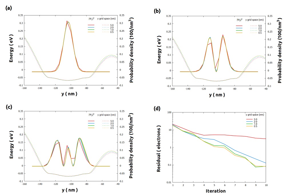
Figure 285 Results of the self-consistent Schrödinger-Poisson simulations using different grid spacing in the y-direction only within the reduced QROI (section xz_Si_QDs). (a) -(c) wavefunctions (solid lines) for the three lowest states overlapped with the conduction band (dotted lines) (d) residual evolution.
These are intermediate results after only 10 iterations: the convergence process was still not completed.#
The evolution of the residuals are very similar, except for the case of 5 nm.
Additionally, for $space_y_QR of 1 nm or less the wavefunctions are smooth and do not present relevant changes.
Repeating a similar procedure for different grid resolutions in the x-direction ($space_x_QR) we obtain the wavefunctions of the Figure 286.
In the y-direction the grid resolution in this region was considered equal to 1 nm ($space_y_QR = 1 in our input file).
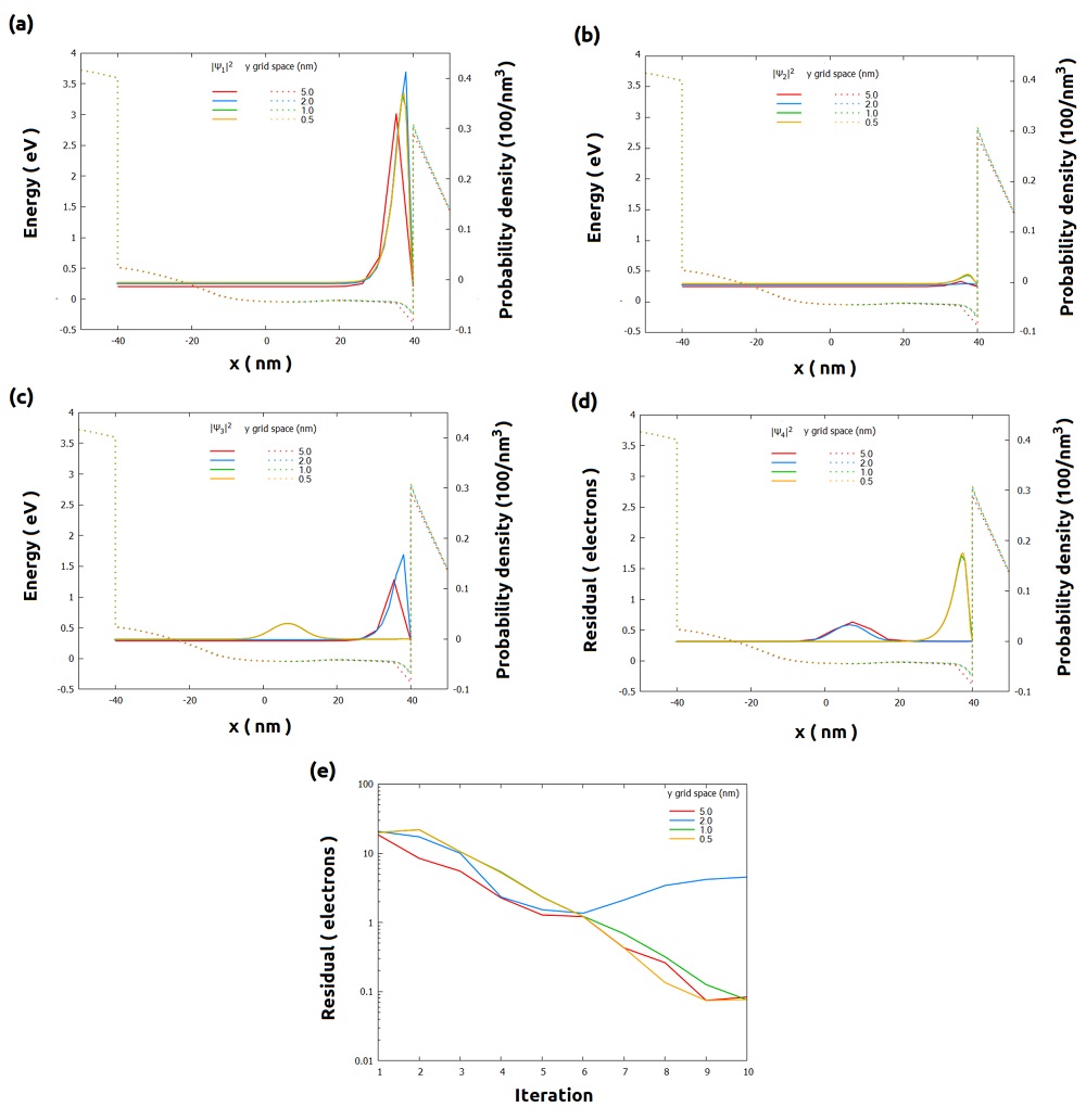
Figure 286 Results of the self-consistent Schrödinger-Poisson simulations for section yz_Si_QDs using different grid spacing in the x-direction within the QROI: (a)-(d) wavefunctions (solid lines) for the four lowest states overlapped with the conduction band (dotted lines), and (e) residual evolution.
These are intermediate results after only 10 iterations: the convergence process was still not completed.
$space_y_QR was kept 5 nm.#
From analysis of these plots, we observe that decreasing the grid resolution in the x-direction from 1 nm to 0.5 nm does not introduce significant improvement in the computation of the density of probabilities from the wavefunctions in the first 10 iterations.
For this reason, we infer that values of 1 nm or less for $space_x_QR and $space_y_QR will be required for more accurate simulations.
4. Expanding the Quantum Region: time to get beautiful plots (and accurate results)!#
Using the results obtained for reduced QROI, we can now design the whole quantum region, now extended from -150 nm to 150 nm for the y-direction.
Until now the central valley of the conduction band in Figure 282 (around y = 0) was not part of the reduced QROI.
Therefore, it may require to increase the number of the eigenvalues in the self-consistent computations in order to fill also this region with carriers.
How to estimate the minimum number of eigenvalues required ($Nstates)?
Our hint is to use, once again, our lower resolution grid within the quantum region (for example, with 5 nm) and few iterations (10) for this tuning. We will reserve the finer grid (1 nm) we previously obtained, only to get the final accurate results. Figure 287 illustrates a sequence of simulations where the grid resolution and the number of states were iteratively changed.
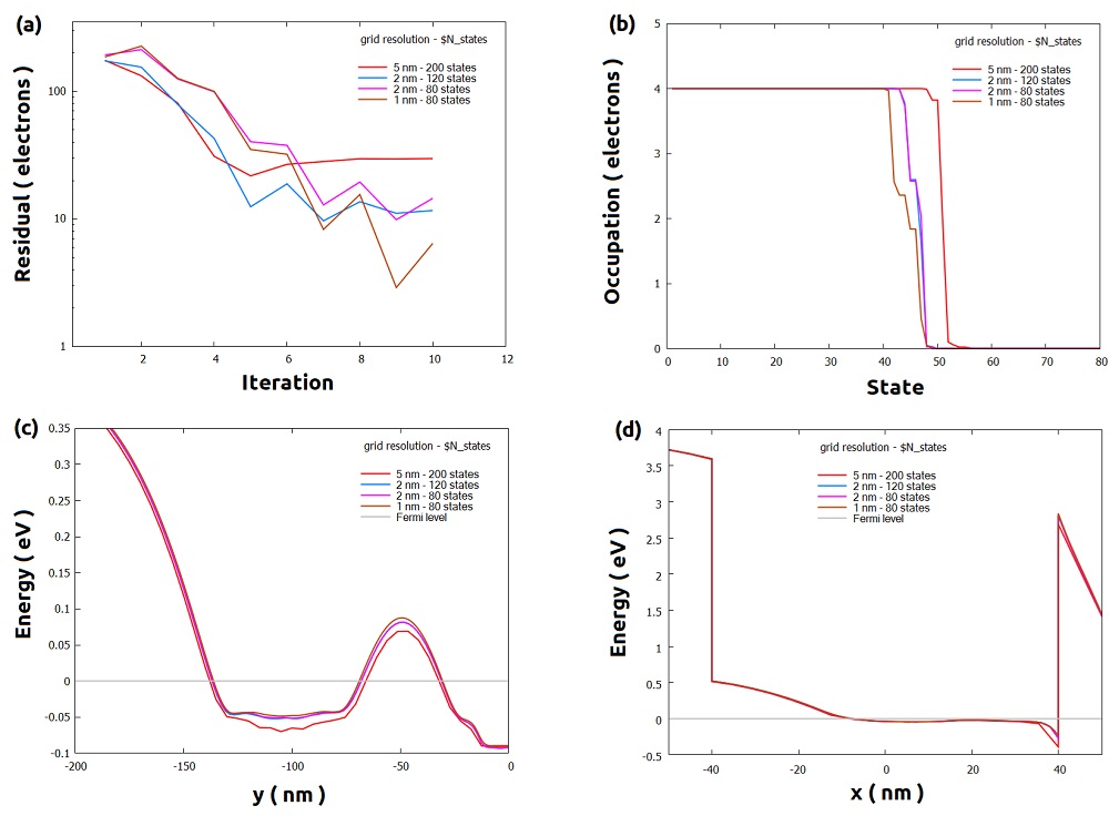
Figure 287 Sequence of simulations for defining a suitable value for $Nstates. (a) residual evolution, (b) occupation number of the most populated band, (c) and (d) conduction band for the sections xz_Si_QDs and yz_Si_QDs, respectively.
These are intermediate results (only 10 iterations of the coupled solvers were taken into account).#
From the coarser grid we observed that the occupation number in the most populated band it is no more than 80 states. The residual of the density of electrons decreases as the grid gets finer and the number of states is around 80. The conduction band in the more relevant sections, shown in the image, does not change too much, for grid spacing less than 2 nm in the quantum region.
Now it is time to obtain more accurate results.
As we mentioned before we will compute 80 states in a quantum grid with $space_x_QR = 1 and $space_y_QR = 1.
The convergence process will be controlled by the maximum number of iterations ($quantum_iterations = 100) and the accuracy desired ($CRes) for the residual of the quantum densities.
The solutions converge when the quantum density of electrons is smaller than Cres before ending the total number of iterations of the self-consistent calculations.
We start, for example, with a constraint $CRes = 1 and, gradually we decrease until the solutions do not change.
Figure 288 shows an example how to choose a suitable value for $CRes.
This corresponds to simulations that converged in less than 100 iterations.
The curves correspond to some wavefunctions for the section xz_Si_QDs when requesting accuracy of 0.1, 0.01 and 1.0.
We observe that the lowest states (like shown in (a)) are more requires more deep constraints in the value of $CRes than the highest states.
Nevertheless, decreasing this parameter from 0.10 to 0.01 does not present a significant improvement in the results.
What you need to keep in mind is which of both values to use: using $CRes = 0.01 will produce, in thesis, better results, but it will result in longer runtimes and more memory for storing the results.
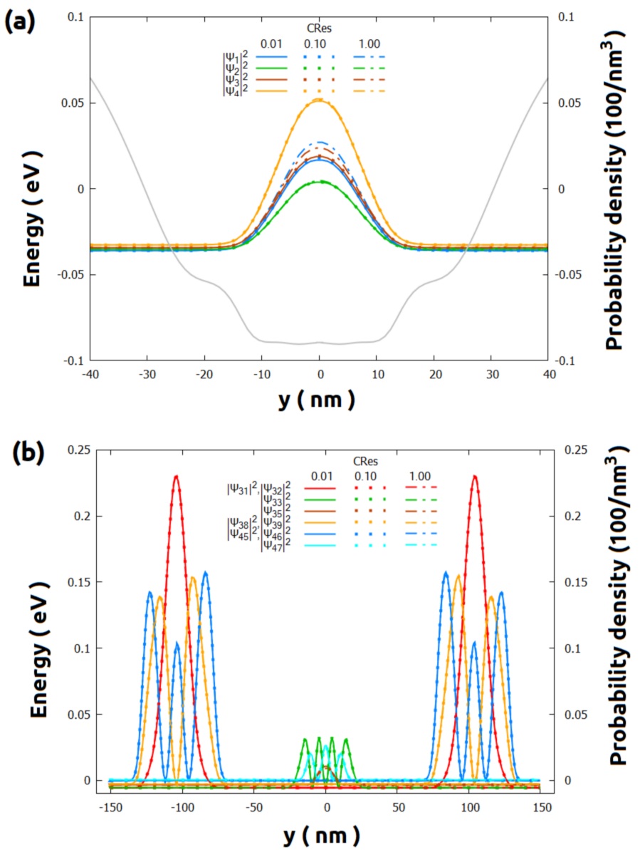
Figure 288 Some wavefunctions in the section xz_Si_QDs as function of the residual used in the convergence process $CRes. (a) in the central, and (b) in the whole quantum region.
All solutions converged before reaching the maximum number of iterations (100).#
The solutions for the section yz_Si_QDs are even more robust than the previous one (see Figure 289): the wavefunctions do not present relevant variation even when the value of $Cres is higher.
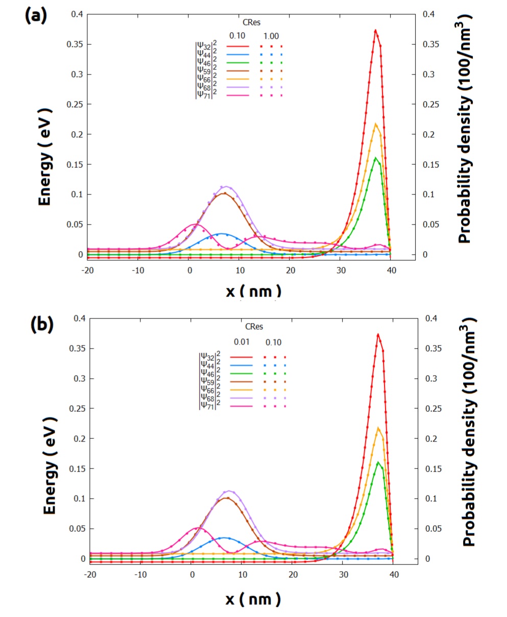
Figure 289 Comparison of some wavefunctions in the section yz_Si_QDs for convergence residual ($Cres) (a) from 1.00 to 0.10, and (b) from 0.10 to 0.01.
All solutions converged before reaching the maximum number of iterations (100).#
Hint
Requiring higher accuracy of the solutions may result in large runtime, when the decrease of residuals are too slow, or even the process does not converge within the chosen maximum number of iterations. Therefore, it is a good practice tracking the residual evolution during the simulations. If they are taking too long (compared with another previous one) for decreasing, you always can interrupt the calculations pressing the key F11 or F12.
Final considerations#
Last but not least, we will simply mention here some important topics are worth to be discussed in separated tutorials.
For some problems that requires really fine grids in very large regions the memory may become the bottleneck of the simulations: the system to be solved may not fit in your RAM. For these situations we implemented in nextnano++ the decomposition method, that converts the 3D-Schrödinger-Poisson problem in multiples 1D problems. Additionally, our implementation results very fast. Nevertheless, this algorithm has intrinsic assumptions, that may not apply to all devices and shall be carefully used. For more detail look at in our page splitquantum{ region{ quantize_x{ }, … } } of our documentation.
Nevertheless, this algorithm has intrinsic assumptions, that may not apply to all devices and shall be carefully used.
It is also important to mention that, coherent quantum transport calculations can be performed using the nextnano++ implementation of the CBR method. The performance of these computations can be improved implementing small changes in the final input file from this tutorial. The most important modification consists on importing the file with the final result of the electrostatic potential from your self-consistent simulations, instead of being solved directly. Our tutorial Landauer conductance and conductance quantization: from quantum wires to quantum point contacts presents this method in detail and the corresponding input files than can be easily extended to 3D devices.
One again, we remind you that in this tutorial we considered only a combination of biases applied to the gates. It is always convenient to check the constraints (boundary conditions for the quantum region, occupation number, residual evolution, etc.) to another scenarios.