
Subband occupations of 2DEG InGaAs/InAlAs HEMTs#
Last update: 2026-04-27
- Files for the tutorial located in nextnano++\examples\transistors
zb_III-V_InGaAs-AlGaAs_2DEG_occupation_1D.nnp
- Important output files
bias_00000/bandedges.datbias_00000/Quantum/2DEG/kp8/probabilities_shift_k00000.datbias_00000/Quantum/2DEG/kp8/density_subbands.datbias_00000/Quantum/2DEG/kp8/occupation.datbias_00000/Quantum/2DEG/Gamma/probabilities_shift_k00000.datbias_00000/Quantum/2DEG/Gamma/density_subbands.datbias_00000/Quantum/2DEG/Gamma/occupation.dat
Occupation of subbands in 2DEGs manifests in the Shubnikov-de Haas effect, which can be measured experimentally. This tutorial shows how to calculated charge densities of each subband and their integrals in an AlInAs/InGaAs/AlInAs HEMT heterostructure (see the Table 18) using different band models. It also highlights importance of the choice of the band model for obtaining accurate solutions.
Name |
Material |
thickness (nm) |
doping (1019cm-3) |
|---|---|---|---|
Schottky Layer |
Al0.5In0.5As |
20 |
— |
Delta doping |
Al0.5In0.5As |
3 |
2.80 |
Spacer |
Al0.5In0.5As |
7 |
— |
Quantum Well |
In0.5Ga0.5As |
20 |
— |
Buffer |
Al0.5In0.5As |
50 |
— |
Poisson and Schrödinger equations are solved self-consistently in 1D. Boundary conditions for the electrostatic potential are default for in the buffer (Neumann) and Dirichlet at the beginning of the Schottky layer, the Schottky contact. They are imposed by choosing a specific Schottky barrier. Dirichlet boundary conditions are used for the Schrödinger equation. The region within which this equation is solver spans from the left boundary of the simulation domain until about 5 nm into the buffer. Strain effects are included within pseudomorphic model.
Two confining regions can be observed in this system. The most important one is at the right edge of the quantum well region, where the 2DEG of interest is formed. A triangular potential is formed there due to electrostatic effect introduced by the delta doping. If the doping was not present, then square quantum well would be present. At the position of the delta doping there is a second confining potential. As it falls below the Fermi level, it is a potential source of a parallel channel, later shown to be negligible in this case.
As the Fermi level is far away from the valence bands and the temperature of the system is set to 2 K, the hole states can be completely neglected in the simulation. Due to low temperature, only the electron state below the Fermi level are occupied and contribute to the charges. Therefore, one needs to calculate subband densities only for these conduction subbands of which minimum is falling below the Fermi level. These are the first 3 bands, in the case of th 1-band model, which implicitly assumes spin degeneracy for every computed state. One needs to calculate and 6 subbands within 8-band \(\mathbf{k} \cdot \mathbf{p}\) model to get an equivalent description of the system.
Even though the band gap in this heterostructure is always at least around 1 eV, and no holes are present, inclusion of the valence band in the band model leads to qualitatively different results. It is due to non-parabolic shape of the electronic band structures of bulk-materials, arising from the interaction between the valence and conduction bands. In this specific example, one can see that 1-band model shows the 3rd band occupied. This one is with states localized in the parallel channel, which is undesired. At the same time the 8-band model shows that only two subbands (four in terms of 8-band model) are occupied, all in the QW region. This can be seen in the Figure 190.
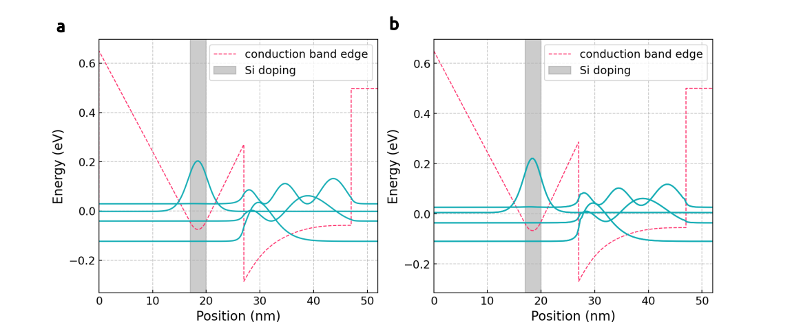
Figure 190 Energy profiles of the HEMT heterostructure with 2DEG with probability densities of the states at the subbands minima obtained within (a) 1-band model, and (b) 8-band \(\mathbf{k} \cdot \mathbf{p}\) model. The gray area in the band diagram marks the Si \(\delta\)-doped region.#
While calculating contribution of these subbands with 1-band model does not require further attention, using \(\mathbf{k} \cdot \mathbf{p}\) method requires defining parameters controlling the integrating states over the selected part of the first Brillouin zone.
Please follow instructions in the section: How to set attributes in k_integration{} - integrating over the FBZ to do so.
Once done, contribution of each band to the total charge density can be outputted simply using the keyword output_subband_densities{ } to files bias_00000Quantum2DEGGammadensity_subbands.dat and bias_00000Quantum2DEGkp8density_subbands.dat, depending on the choice of the model.
As shown in the Figure 191, 1-band model predicts the parallel channel while 8-band model does not.
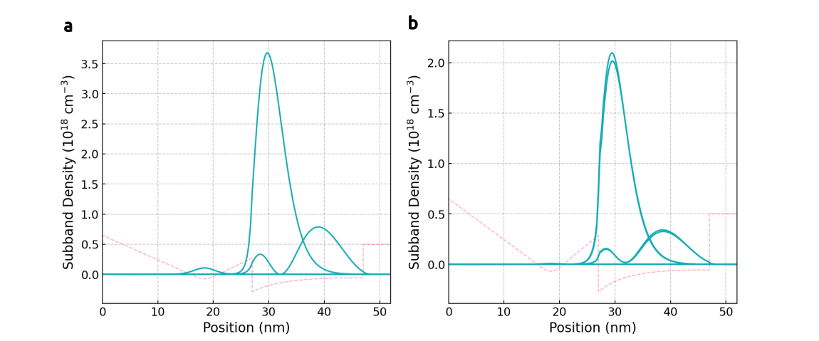
Figure 191 The calculated subband densities within (a) 1-band model, and (b) 8-band \(\mathbf{k} \cdot \mathbf{p}\) model. Energy profile of the conduction band is provided just for reference.#
Finally, in practice, one needs only the integrals of these densities over the reals space for each subband separately for the analysis of the Shubnikov-de Haas effect.
These numbers can be always found in the files bias_00000Quantum2DEGGammaoccupation.dat and bias_00000Quantum2DEGkp8occupation.dat, depending on the choice of the model.
Note that the occupations of the \(\mathbf{k} \cdot \mathbf{p}\) bands are approximately twice smaller in the absolute value.
It is due to lack of implicitly imposed double degeneracy of the bands, which is always present in 1-band models.
Also, it is rare that bands are fully double degenerate in semiconductor heterostructures, hence slight deviations of the occupation between pairs of the bands within \(\mathbf{k} \cdot \mathbf{p}\) model are justified.
Band number |
Occupation |
|---|---|
1 |
2.331e+12 |
2 |
7.667e+11 |
3 |
5.224e+10 |
4 |
1.703e-64 |
Band number |
Occupation |
|---|---|
1 |
1.260e+12 |
2 |
1.229e+12 |
3 |
3.518e+11 |
4 |
3.372e+11 |
5 |
1.132e-77 |
6 |
3.111e-78 |
7 |
5.805e-164 |
8 |
3.404e-167 |
- Acknowledgments
This tutorial was created in cooperation with Eleftherios Skuras, Associate Professor at Department of Electrical and Computer Engineering, University of Patras.
This site is co-funded by European Union within the project CHIPS of Europe connecting universities and industry to train the next generation of semiconductor experts.