

Energy dispersion of holes in a quantum well#
Last update: 2026-05-19
- Files for the tutorial located in nextnano++\examples\electronic_band_structures
1Dwell_GaAs_AlAs.nnp1Dwell_GaSb_AlSb.nnp1Dwell_InGaAs_InP.nnp
- Files for the tutorial are not available yet
1DIn20Ga80AsQW_75nm_sg.nnp1DIn20Ga80AsQW_75nm_kp.nnp1DIn20Ga80AsQW_75nm_kp_dispersion.nnp
Contents
Introduction#
In this tutorial we aim to reproduce results of [FranceschiJancuBeltram1999] and [Holleitner2007].
a) Unstrained \(GaAs/ AlAs\) quantum well#
Input file: 1Dwell_GaAs_AlAs.nnp
This input file simulates a GaAs (well)/ AlAs (barrier) structure - The well is 17 molecular layers thick (4.8 nm), located between \(x\) = 20 nm and \(x\) = 24.8 nm.
Figure 121 shows the valence band edges of the quantum well structure together with three quantized states. The heavy and light hole band edges are degenerate. The red band is the split-off hole band edge. Note that these artificial band edges correspond to the bulk band edges. Also shown are the probability densities of the three uppermost subbands (\(\Psi^2\)). Note that each eigenstate is twofold spin-degenerate at \(k_{||}\) = 0. These eigenfunctions are plotted as positions on the energy scale that correspond to their eigenenergies, i.e. \(\Psi^2\) + eigenvalue (eV). The energy scale is shifted by -1.45967 eV to refer to the bulk valence band edge of the quantum well material, i.e. the GaAs valence band edge (hh, lh) is at 0 eV.
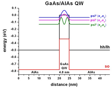
Figure 121 Calculated valence band edges with \(\Psi^2\) of the lowest hole states.#
We use a 6-band k.p model for the holes.
quantum {
    region{
        name = "quantum_region"
        x = [10, 34.8]
        no_density = yes
        boundary{ x = dirichlet }
        kp_6band{ # 6-band k.p model
            num_ev = 10 # number of hole states
            dispersion{
                ...
            }
            k_integration{
                ...
            }
        }
        output_states{ # k.p output
            max_num = 9999
            all_k_points = yes
            amplitudes = no
            probabilities = yes
        }
    }
}
Database: We used the Luttinger parameters (\(\gamma_1\), \(\gamma_2\), \(\gamma_3\)) given in [FranceschiJancuBeltram1999] and also their valence band offset (0.5 eV).
The conversion from Luttinger parameters to Dresselhaus parameters (L, M, N) is described here.
For details on the band offset see Definition of band offsets (zincblende).
So the changes to the database.nnp file are as follows:
database{
    binary_zb{
        name    = AlAs
        valence = III_V

        valence_bands{
            bandoffset = 0.86633 # Ev,av [eV]
        }

        kp_6_bands{     # Dresselhaus parameters
            L = -7.64   # [hbar^2/2m]
            M = -3.50   # [hbar^2/2m]
            N = -8.76   # [hbar^2/2m]
        }
    }

    binary_zb{
        name    = GaAs
        valence = III_V

        valence_bands{
            bandoffset = 1.346 # Ev,av [eV]
        }

        kp_6_bands{     # Dresselhaus parameters
            L = -16.050 # [hbar^2/2m]
            M = -4.050  # [hbar^2/2m]
            N = -18.000 # [hbar^2/2m]
        }
    }
}
The valence band offset between InAs and GaAs is 0.5 eV [FranceschiJancuBeltram1999] and calculated as follows:
\(k_{||}\) dispersion for the three uppermost subbands#
The eigenvalues are twofold degenerate due to spin (and because the quantum well is symmetric). Thus, eigenvalue 1 and 2 correspond to Figure 122, 3 and 4 to Figure 123 and 5 and 6 to Figure 124. For the following three pictures, the energy is referred to the bulk valence band edge of the quantum well material, i.e. hh/lh(GaAs) = 0 eV. The colors and the color bar correspond to the energy given in eV. The \(x\) and \(y\) coordinate axes refer to the in-plane wave vector. The units are in 1/Angstrom.
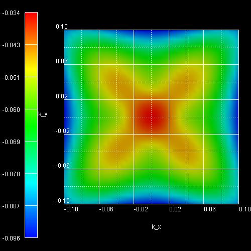
Figure 122 Subband 1 (eigenvalue 1 and 2)#
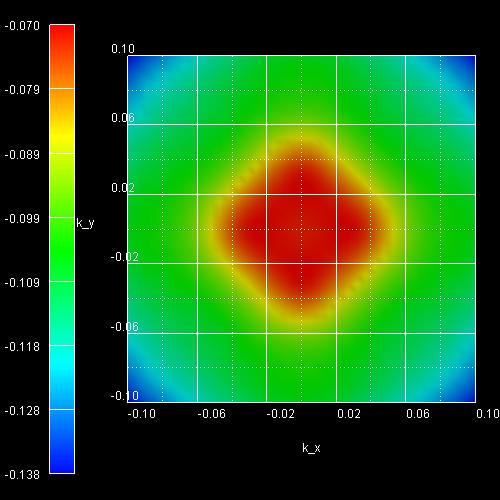
Figure 123 Subband 2 (eigenvalue 3 and 4)#
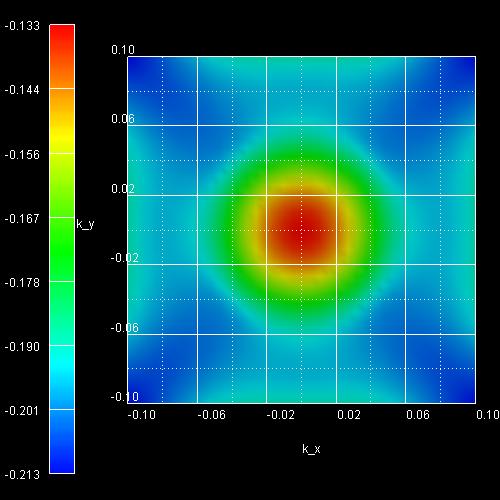
Figure 124 Subband 3 (eigenvalue 5 and 6)#
Now we will plot a cut through the above three pictures from [010] to the zone center and from the zone center to [011], see Figure 125.
This plot was obtained by plotting the following file: dispersion_quantum_region_kp6_kpar_10_00_11.dat.
The value of the abscissa is found as follows:
From [10] to zero we just take \(-k_x\).
From zero to [11] we take \(\sqrt{k_x^2+k_y^2}\).
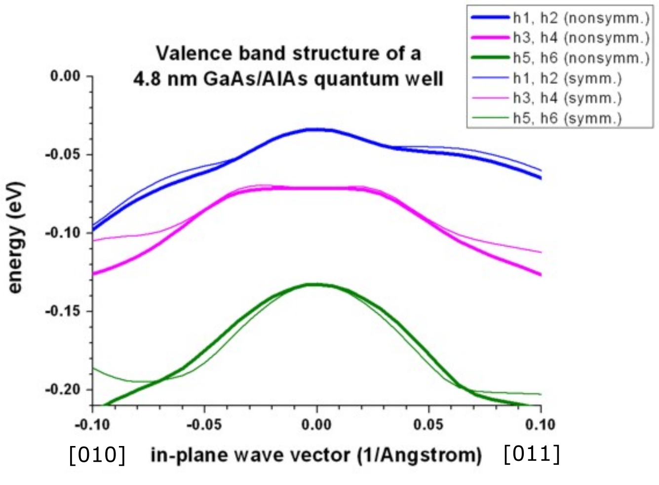
Figure 125 Calculated valence band structure of a \(GaAs/ AlAs\) QW.#
The above figure shows the eigenvalues as a function of \(k_{||}\) vector. The three lines correspond to the upper three eigenvalues (which are two-fold spin-degenerate) as shown in the above QW figure. The thick lines are for the nonsymmetrized k.p Hamiltonian (which is closer to the more accurate tight-binding results), the thin lines are for the symmetrized k.p Hamiltonian. The two sets of k.p subbands coincide at the Brillouin-zone center (i.e. at \(k_{||}\) = 0). They do not show pronounced discrepancies at nonzero in-plane \(k\) vectors. This follows from the rather small difference between the effective-mass parameters of GaAs and AlAs. Obviously, for larger \(k\) values, the discrepancies are more significant.
b) Tensely strained \(GaSb/ AlSb\) quantum wells#
Input file: 1Dwell_GaSb_AlSb.nnp
Figure 126 reproduces Fig. 2 of [FranceschiJancuBeltram1999] very well. It is a tensely strained 5.1 nm GaSb quantum well embedded between unstrained AlSb barriers. The biaxial strain is 0.65 % and breaks the degeneracy of the bulk heavy and light hole band edge. Now the light hole band edge lies above the heavy hole band edge.
The figure shows that the first two subbands are nearly degenerate at the Brillouin zone center and show strong coupling.
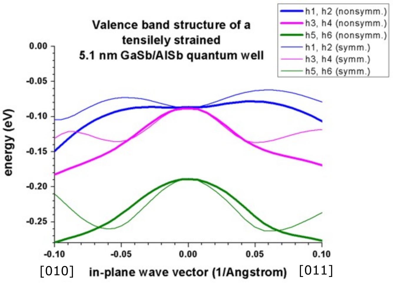
Figure 126 Calculated valence band structure of a tensely strained \(GaSb/ AlSb\) QW.#
A large discrepancy between the nonsymmetrized and the symmetrized k.p Hamiltonian can be seen. (See also the discussion in [FranceschiJancuBeltram1999] and their tight-binding results.)
c) Tensely strained \(In_{0.43}Ga_{0.57}As/ InP\) quantum wells#
Input file: 1Dwell_InGaAs_InP.nnp
The following figure reproduces Fig. 3 of [FranceschiJancuBeltram1999] very well. It is a tensely strained 5.7 nm \(In_{0.43}Ga_{0.57}As\) quantum well embedded between unstrained InP barriers. The biaxial strain is 0.73 % and breaks the degeneracy of the bulk heavy and light hole band edge. Now the light hole band edge lies above the heavy hole band edge.
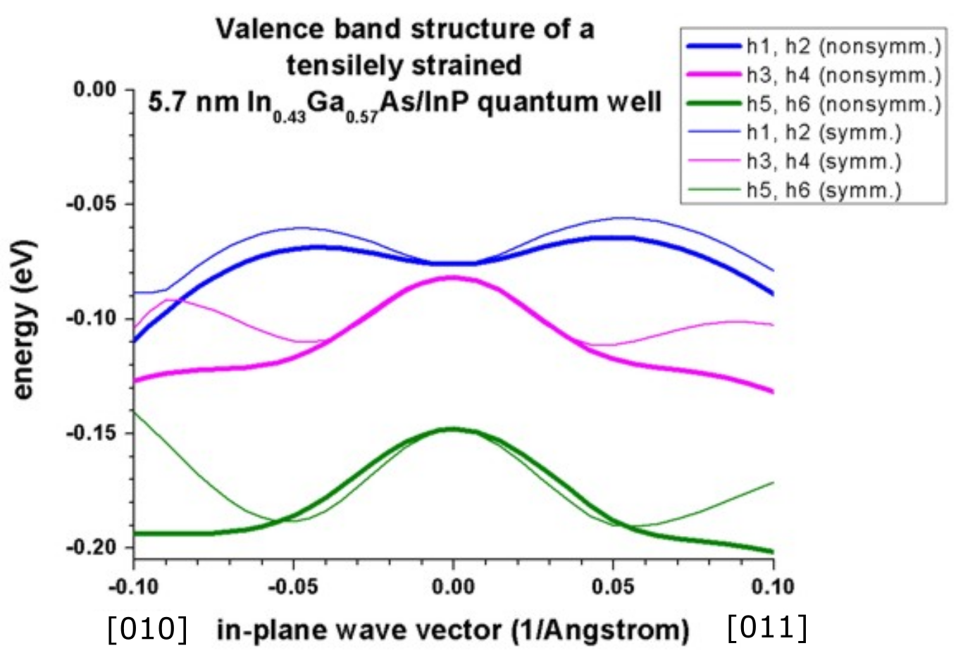
Figure 127 Calculated valence band structure of a tensely strained \(In_{0.43}Ga_{0.57}As/ InP\) QW.#
Again, a large discrepancy between the nonsymmetrized and the symmetrized k.p Hamiltonian can be seen. (See also the discussion in [FranceschiJancuBeltram1999] and their tight-binding results.)
d) Strained \(In_{0.2}Ga_{0.8}As/ GaAs\) quantum well#
The input files used below have been used for Fig. 8 in the following paper: [Holleitner2007].
1DIn20Ga80AsQW_75nm_sg.nnp#
A 7.5 nm \(In_{0.2}Ga_{0.8}As\) quantum well is sandwiched between two GaAs layers. The quantum well is grown pseudomorphically on a GaAs substrate and is thus strained compressively with respect to the GaAs substrate.
The GaAs is n-type doped with Si with a concentration of 3 \(\cdot\) 1017 cm-3 in the regions between \(x\) = 50 nm and \(x\) = 80 nm and between \(x\) = 127.5 nm and \(x\) = 137.5 nm.
Consequently, we first have to solve the single-band Schrödinger equation together with the Poisson equation self-consistently, in order to obtain the electrostatic potential. The electron ground state is below the Fermi level.
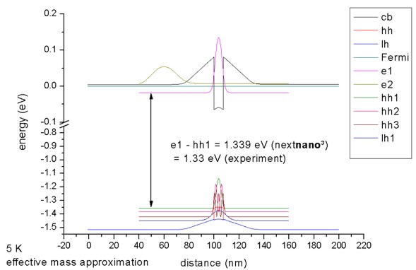
Figure 128 Calculated band edge profile of a compressively strained \(In_{0.2}Ga_{0.8}As/ GaAs\) QW (single-band Schrödinger equation).#
1DIn20Ga80AsQW_75nm_kp.nnp#
The calculated electrostatic potential is read in and then the 8-band k.p equation is solved to get the eigenstates for \(k_{||}\) = 0. The calculated transition energy between the ground state electron and the ground state (heavy) hole is 1.340 eV. (Note: The exciton correction has not been considered and is of the order 4 meV.)
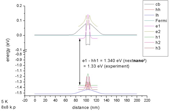
Figure 129 Calculated band edge profile of a compressively strained \(In_{0.2}Ga_{0.8}As/ GaAs\) QW (8-band k.p).#
For \(k_{||} = 0\), the three highest hole states have heavy hole character whereas the forth state has light hole character. No further states are confined. The split-off hole band edge is far away from the heavy and light hole band edges (~ 0.3 eV).
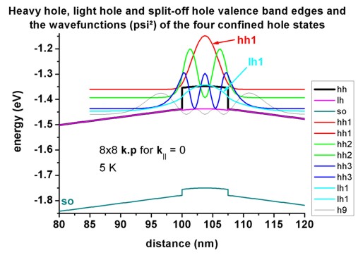
Figure 130 Calculated valence band structure and lowest hole states of a compressively strained \(In_{0.2}Ga_{0.8}As/ GaAs\) QW (8-band k.p).#
1DIn20Ga80AsQW_75nm_kp_dispersion.nnp#
We read in the electrostatic potential again and calculate the 8-band k.p dispersion for \(k_{||}\neq 0\). This time the calculation is more time-consuming as the Schrödinger equation has to be solved for 250 different \(k_{||}\) points, i.e. the CPU time is 250 times larger than for \(k_||\) = 0 only.
For \(| k_{||} |\) <= 0.02 1/Angstrom, the directions [10] and [11] are practically identical for the uppermost hole level, see Figure 131.
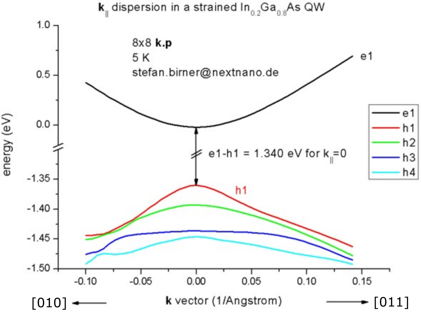
Figure 131 Calculated subband dispersions in \(In_{0.2}Ga_{0.8}As/ GaAs\) QW.#
Figure 132 shows the \(k_{||}\) dispersion of the highest hole state (h1). The \(x\) axis shows the kx value between -0.10 [1/Angstrom] and 0.10 [1/Angstrom], the \(y\) axis shows \(k_y\). The maximum energy of the hole state occurs at -1.3603 eV at (\(k_x\), \(k_y\)) = (0, 0), i.e. in the center of the figure (Gamma point).
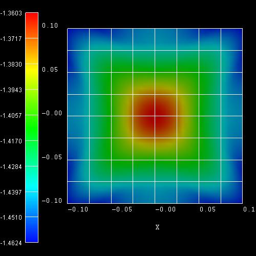
Figure 132 Calculated dispersion of h1 state in a \(In_{0.2}Ga_{0.8}As/ GaAs\) QW.#