

Electronic band structure of a trilayer InAs/GaxIn1-xSb/InAs quantum well#
Last update: 2026-06-02
This validation shows that our software can reproduce the electronic band dispersion of a trilayer InAs/GaxIn1-xSb/InAs quantum well using 8-band \(\mathbf{k} \cdot \mathbf{p}\) method, qualitatively reproducing the Figure 1. (D) from [Meyer2025] and the Figure S1 (B) from supplementary materials to this publication. The simulation is defined based on the input files from InAs/GaxIn1-xSb/InAs: triple quantum well for topological electronics.
Files#
Files available within premium support:
Meyer_2025_trilayer_quantum_well_InAs_GaInSb_1d.nnpMeyer_2025_script.py- (NOT AVAILABLE YET) a Python script facilitating comparison with the reference data*.dat- files containing digitalized data of the figure S1 (B) from [König2008]
Results#
[Meyer2025] reports a gap of 27 meV, while our numerical simulations yield a value of 22.5 meV. This corresponds to an acceptable deviation of approximately 4.5 meV (\(\approx\) 17%). Panel (b) of Figure 538 illustrates the energy bands E1, E2, and H2 of the trilayer quantum well.
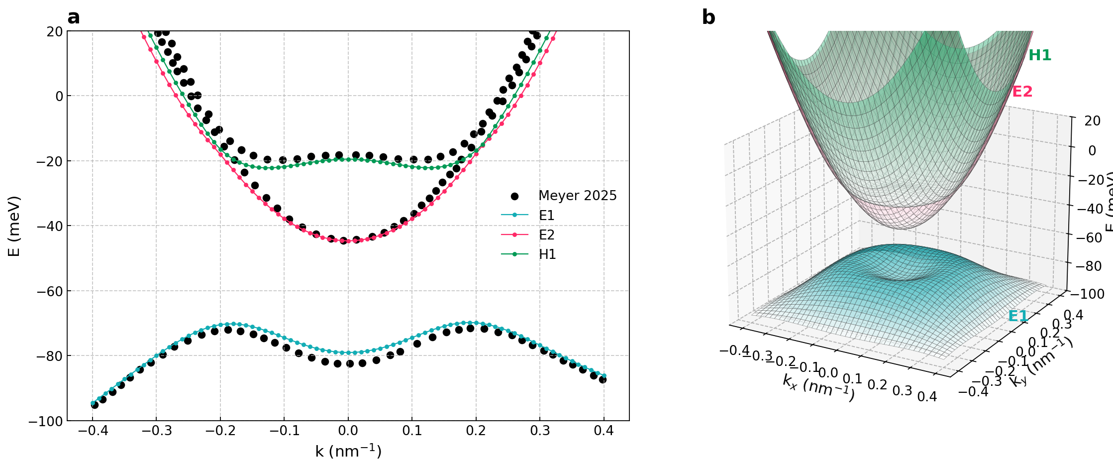
Figure 538 (a) Energy bands E1, E2, and H2 of the tri-layer QW. (b) 3D surfaces of E1 and E2 bands of the tri-layer QW. The indirect gap (\(\approx 25 \text{ meV}\)) is governed by the energy split between the bands E2 and E1.#