
Band gap of strained AlGaInP on GaAs substrate#
Last update: 2026-04-21
- Files for the tutorial located in nextnano++\examples
AlGaInP_on_GaAs_1D.nnp
- Important output files
strain/strain_simualtion.datstrain/hydrostatic_strain.datbias_00000/bandedges.dat
Contents
Introduction#
In this tutorial we study the band gaps of strained \(Al_xGa_yIn_{1-x-y}P\) on a GaAs substrate. The material parameters are taken from [VurgaftmanJAP2001].
Strain#
To understand the effect of strain on the band gap on the individual components of the quaternary \(Al_xGa_yIn_{1-x-y}P\), we first examine the effects on
AlP strained tensely with respect to GaAs
GaP strained tensely with respect to GaAs
InP strained compressively with respect to GaAs
\(Al_xGa_{1-x}P\) strained tensely with respect to GaAs
\(Ga_xIn_{1-x}P\) strained with respect to GaAs
\(Al_xIn_{1-x}P\) strained with respect to GaAs
\(Al_{0.4}Ga_{0.6}P\) strained tensely with respect to GaAs
\(Ga_{0.4}In_{0.6}P\) strained compressively with respect to GaAs
\(Al_{0.4}In_{0.6}P\) strained compressively with respect to GaAs
Each material layer has a length of 10 nm in the simulation. The material layers 4), 5) and 6) vary their alloy contents linearly, i.e.
\(Al_xGa_{1-x}P\): x = 0.0 to x = 1.0 (from 10 nm to 20 nm)
\(Ga_xIn_{1-x}P\): x = 0.0 to x = 1.0 (from 30 nm to 40 nm)
\(Al_xIn_{1-x}P\): x = 1.0 to x = 0.0 (from 50 nm to 60 nm)
There is no external stress applied to the structure, so Poisson’s ratio holds. All layers are strained pseudomorphically with respect to a GaAs substrate (i.e. the layers are biaxially strained in the plane perpendicular to the growth direction to match the lattice constant of GaAs).
The biaxial strain in the layers can be calculated with this formula:
where \(a\) is the lattice constant. The output of the strain tensor can be found in this file:
strain/strain_simualtion.dat
The hydrostatic strain is the trace of the strain tensor and corresponds to the volume deformation:
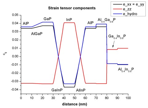
Figure 34 Strain tensor components#
band gaps#
Figure 35 shows the conduction band edges at the Gamma, L and X points and the heavy hole, light hole and split-off hole valence bands. The red line shows that band gap, i.e. the difference between the lowest conduction band minimum and the valence band maximum. The band gap maximum occurs at \(Al_{0.55}In_{0.45}P\) (2.355 eV).
The conduction and valence band edges have been obtained taking into account the shifts and splittings of the bands due to strain and deformation potentials.
Note that conduction and valence band offsets are not taken into account in this plot. The zero of energy was taken to be the unstrained heavy hole / light hole band edge.
Due to strain, the degeneracy of the heavy and light hole is lifted. Also, the X band splits into two X bands (2-fold and 4-fold degeneracy).
In the case of tensile (compressive) strain, the light (heavy) hole band is the valence band maximum.
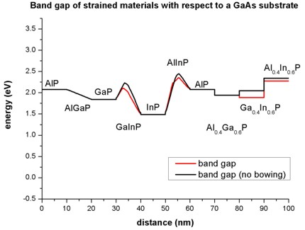
Figure 35 Band edge and band gap profile#
Note that the material parameters include band gap bowing.
Figure 36 compares the overall band gap to the case where band gap bowing has been neglected.
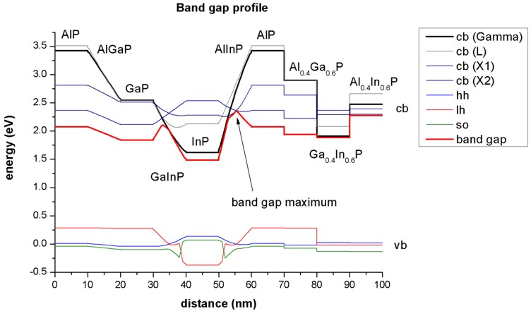
Figure 36 Ban dgap profile#
The nextnano++ tool supports quaternaries:
quaternary_constant{
    name = "Al(x)Ga(y)In(1-x-y)P"
    alloy_x = 0.255
    alloy_y = 0.255
}
Appendix E of the PhD thesis of T. Zibold ([ZiboldPhD2007]) is related to the nextnano++ implementation of quaternaries.