

Resonant tunneling diode (RTD): flat-band model#
Files for the tutorial located in nextnano.NEGF\examples\RTDs:
RTD_zb_III-V.negf
plot_Current_vs_Voltage.plt (Figure 33)
Note
This tutorial reports a simplified approach for RTD simulation. A more realistic method is available for RTD simulation, see Resonant tunneling diode (RTD) simulation using the hybrid method
Parameters
Ballistic– assume ballistic transport between the contacts (i.e., neglect scattering processes in the device)
Output files
Input\Conduction_BandEdge.dat (Figure 25)
Init_Electron_Modes150mV\EnergyEigenstates\EigenStates.dat (Figure 26)
(Bias)mV\2D_plots\DensityOfStates_ZoneCenter.vtr (Figure 27, Figure 28)
(Bias)mV\2D_plots\CarrierDensity_ZoneCenter.vtr (Figure 29, Figure 30)
(Bias)mV\2D_plots\CurrentDensity_ZoneCenter.vtr (Figure 31, Figure 32)
Current_vs_Voltage.dat (Figure 33)
Summary#
The nextnano.NEGF tool can simulate current-voltage characteristics of resonant tunneling diodes (RTDs).
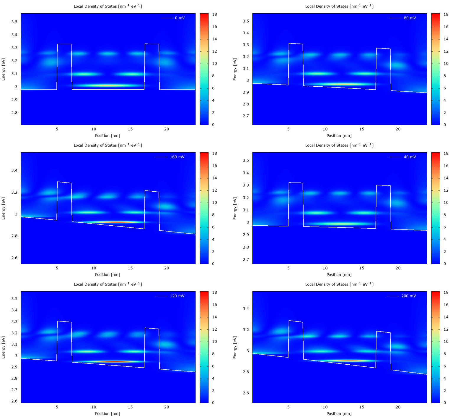
Figure 23 Local density of states in the presence of scattering. (Run Animation_DensityOfStates.plt in the output to reproduce)#
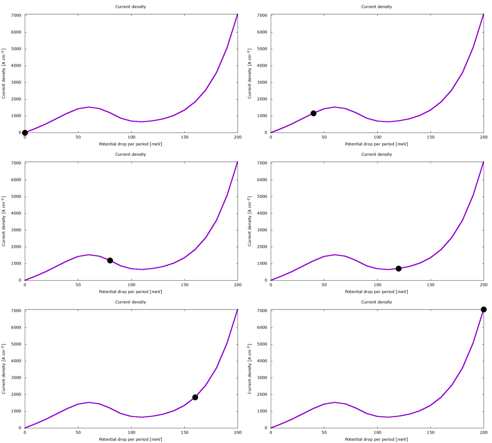
Figure 24 Current-voltage characteristics in the presence of scattering. (Run Animation_Current.plt in the output to reproduce)#
Simulation input#
The first input file takes the scattering mechanisms into account, while the second input file ignores them.
You can use template feature of nextnanomat to sweep the variable Ballistic.
Definition of materials#
The materials used in the structure, GaAs for well and AlGaAs for barrier, are specified in Materials{ }.
It is specified that the effective mass is calculated from the k.p parameters (Material{ EffectiveMassFromKpParameters }). Also, the effective mass is assumed as energy dependent (NonParabolicity) and the model used for the calculation of effective mass is the one for single-band model (NumberOfBands).
The models used for the calculation of the effective mass are described here: Single-band model.
Definition of layers#
Alternating layers consisting of barrier and well are specified in Structure{ }. In this tutorial, the thickness of each layer is 5.0/2.0/10.0/2.0/5.0 (nm) where AlGaAs barrier layers are in bold.
The resulting conduction band edge profile is shown in Figure 25.
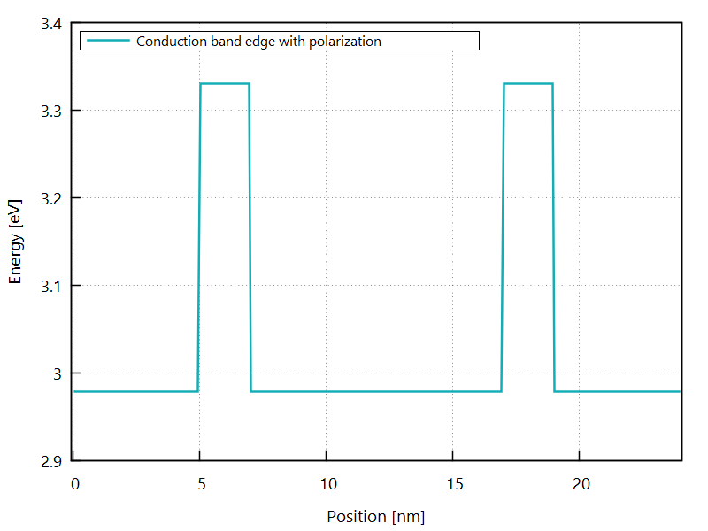
Figure 25 Conduction band edge at zero bias.#
Contacts (open boundary condition)#
In order to simulate a system with open boundary conditions (instead of the default field-periodic boundary condition), contacts have to be defined by adding a Contacts{ } section into the input file.
The keyword Ballistic switches ON/OFF the scattering in the device. Transport between the contacts is assumed ballistic if it is set to yes.
Note
In the version 2020-11-19, only single band calculations are supported for open boundary conditions.
Scattering#
The following scattering mechanisms are included in this tutorial.
Note
In this tutorial, the Coulomb scatterers (ionized impurities and other charge carriers) are assumed to be homogeneously distributed (HomogeneousCoulomb = yes) in order to speed up the calculation.
Note
LO-phonon scattering is applied by default as all materials host LO phonons. The material database contains intrinsic parameters controlling the electron-phonon interaction.
Electrostatics#
The electrostatic mean-field interactions (electron-electron and electron-impurities interactions) is taken into account by Poisson = yes.
In-plane discretization#
The parameters for the LateralDiscretization{ } are taken from the material of well, i.e. GaAs.
Simulation output#
For the overview of output files and folders, see Simulation Output.
Electron eigenstates#
The electron eigenstates of the whole heterostructure are calculated and written to the Init_Electron_Modes150mV\EnergyEigenstates folder. These states are used as the basis states of the Green’s function.
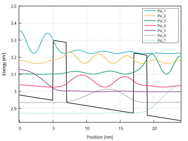
Figure 26 Electron eigenstates for the whole region at the bias of 150 mV.#
Note
There is another output EnergyEigenstates/TightBinding_states.dat that describes the electron eigenstates confined in each GaAs region. These eigenstates are calculated from the Schrödinger equations for each region separated by AnalysisSeparator{ }.
Local density of states#
Figure 27 and Figure 28 show the local density of states (LDOS). Please note that the scaling of the colormap is different in the two figures.
The LDOS tells us where and at which energy electronic states are available that the charge carriers can occupy. The LDOS is shown for \(\mathbf{k}_\parallel=0\), but there are also electronic states available for \(\mathbf{k}_\parallel\neq0\) (see PlotDispersion).
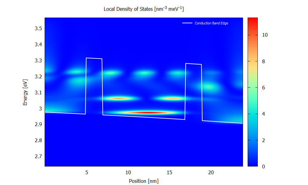
Figure 27 Local density of states calculated with scattering at the bias of 70 mV. (Run 70mV\2D_plots\DensityOfStates.plt to reproduce)#
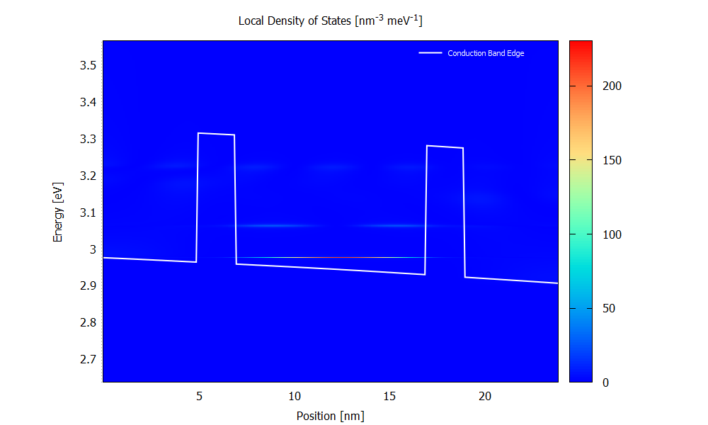
Figure 28 Local density of states calculated with the ballistic condition at the bias of 70 mV. (Run 70mV\2D_plots\DensityOfStates.plt to reproduce)#
Note
The file explorer in nextnanomat does not show the gnuplot (.plt) files. Please access them in your default file explorer.
Electron density#
Figure 29 and Figure 30 show the energy resolved electron density \(n(x,E)\) for the bias of 70 mV. Please note that the scaling of the colormap is different in the two figures.
The electron density is obtained from occupying the LDOS (for both \(\mathbf{k}_\parallel=0\) and \(\mathbf{k}_\parallel\neq0\)) with charge carriers. It is a non-equilibrium occupation that is not described by a Fermi distribution.
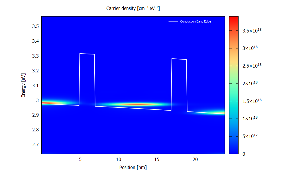
Figure 29 Electron density calculated with scattering at the bias of 70 mV. (Run 70mV\2D_plots\CarrierDensity.plt to reproduce)#
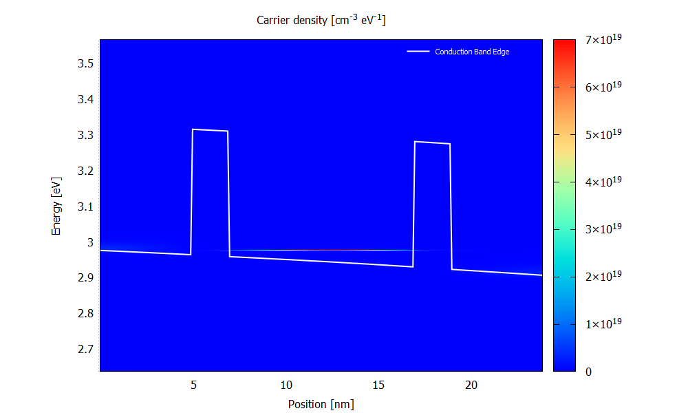
Figure 30 Electron density calculated with the ballistic condition at the bias of 70 mV. (Run 70mV\2D_plots\CarrierDensity.plt to reproduce)#
Current density#
Figure 31 and Figure 32 show the energy resolved current density \(j(x,E)\) for the bias of 70 mV. Please note that the scaling of the colormap is different in the two figures.
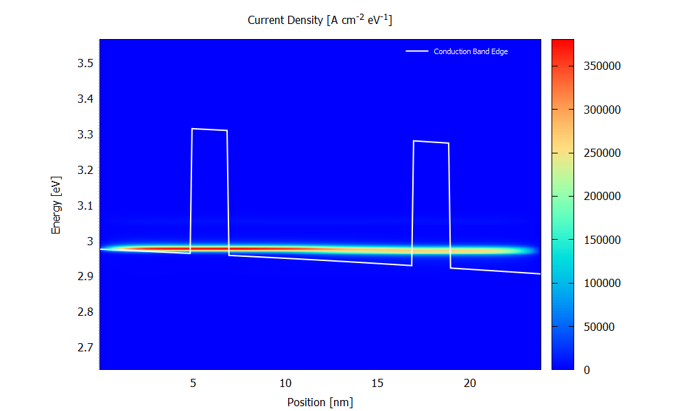
Figure 31 Current density calculated with scattering at the bias of 70 mV. (Run 70mV\2D_plots\CurrentDensity.plt to reproduce)#
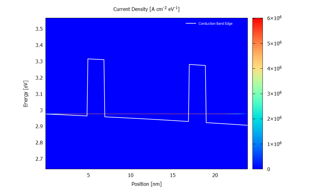
Figure 32 Current density calculated with the ballistic condition at the bias of 70 mV. (Run 70mV\2D_plots\CurrentDensity.plt to reproduce)#
Current-voltage characteristics#
Figure 33 shows the current-voltage characteristics calculated both with and without scattering.
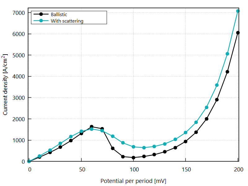
Figure 33 Current-voltage calculated with and without scattering. (Sweep the input file variable Ballistic, copy the *.plt files in the example folder to your output directory, and double-click to reproduce.)#
Last update: 12/11/2024