

Simulation of mid-infrared quantum cascade lasers (QCLs)#
Summary#
This tutorial describes the simulation of the active region of mid-infrared quantum cascade lasers (QCLs) using nextnano.NEGF.
After discussing the input files settings for mid-IR QCLs, the simulation of I-V characteristic and gain spectrum without lasing is presented. In a third part, simulation of lasing above threshold is presented.
All output of simulations are given here for the example [BismutoAPL2010].
Input file settings#
To simulate a mid-infrared QCL, the following sections are needed in the input file:
SweepParameters{ } : defines the voltage sweep range
Temperature : lattice temperature
Crystal{ } : needed for strain-compensated QCLs
Materials{ } : material compositions
Structure{ } : specifies the layer sequence
Scattering{ } : non-radiative scattering parameters
LateralDiscretization{ } : discretization of the in-plane motion
SimulationParameter{ }: general simulation parameters
Output{ } : output settings
Gain{ } : to calculate gain/absorption spectrum
EMfield{ }: for lasing action above threshold
Periodic boundary conditions#
Only the layer sequence of a single period needs be specified in the Structure{ } section.
The field-periodic boundary conditions are activated in the SimulationParameter{ } section, by setting CoherenceLengthInPeriods and nLateralPeriodsForBandStructure to 1 (larger values are not useful for mid-IR QCLs, they will only increase the simulation time).
Electronic structure#
For mid-IR QCLs, the 3-band model is recommended to account for nonparabolicity of the conduction band.
Non radiative scattering mechanisms#
For mid-IR QCLs, the relevant non-radiative scattering processes are:
polar LO phonon scattering: this inelastic scattering is always considered by default, based on material parameters, but can be further tuned using LOPhononCouplingStrength.
Interface roughness scattering: the parameters needs to be specified in InterfaceRoughness{ }
Charged impurity scattering: considered by default, but can be tuned using ImpurityScatteringStrength
Electron-electron scattering: can be activated/deactivated using ElectronElectronScattering
Alloy scattering can be tuned using AlloyScattering
Simulation output#
Initial energy eigenstates#
The first step of the simulation is to solve the Schrödinger equation, which is relatively fast (usually a few seconds). From the computed electronic levels, the low-energy eigenstates are selected and then used to construct the basis used in the NEGF solver.
The output of this step is a plot of the conduction band profile together with the electronic levels. The electronic levels are represented by their probability densities shifted by their energy. The conduction band diagram together with the electronic levels are shown in Figure 8.
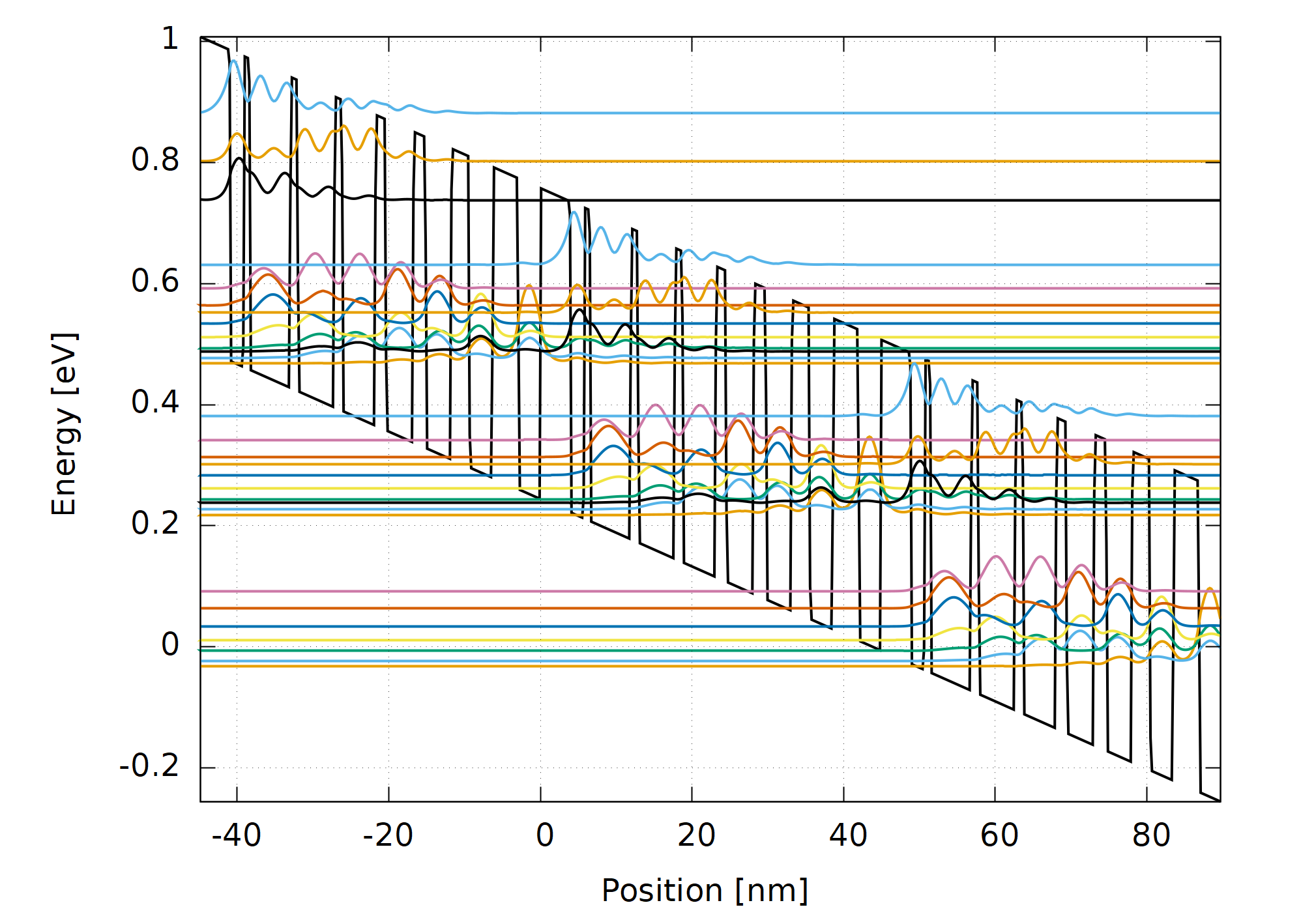
Figure 8 Conduction bandedge and probability densities of the selected electronic levels#
At this initial stage of the simulation, only the Schrödinger equation is solved, without any electrostatic field (i.e. Poisson equation has not been solved yet).
Note that the eigenstates are displayed for a bias that can be specified by the command BiasForInitialElectronicModes. The choice of this bias has no consequence on the following NEGF simulation.
Note
Depending on the axial cut-off energy EnergyRangeAxial, the number of selected subbands varies. Selecting all relevant subbands is important for the accuracy of the NEGF simulation. Yet the NEGF simulation time scales quadratically with the number of selected subbands.
NEGF output#
After convergence of the self-consistent Dyson-Keldysh equations, the Green’s functions contains allows to compute the physical observable. When a sweep is made over multiple bias voltage points, a current-voltage characteristics is obtained as shown in Figure 8.
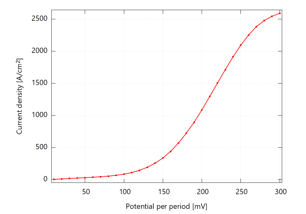
Figure 9 Current-voltage characteristics: current density as a function of voltage drop per period.#
2D plots#
From the retarded and lesser Green’s functions, the energy-resolved carrier density and the local density of states can be respectively extracted. They are shown in Figure 10. The local density of states provides a spatially and energy-resolved information about the availability of quantum states. The 2D plot of carrier density gives the information how these states are actually occupied with electrons.
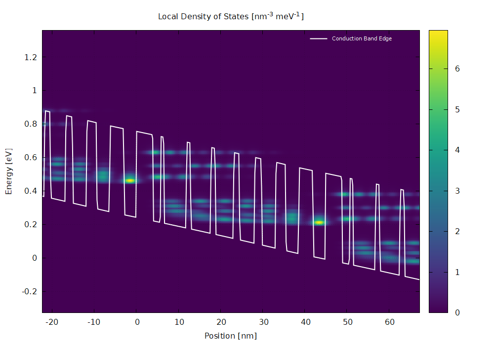
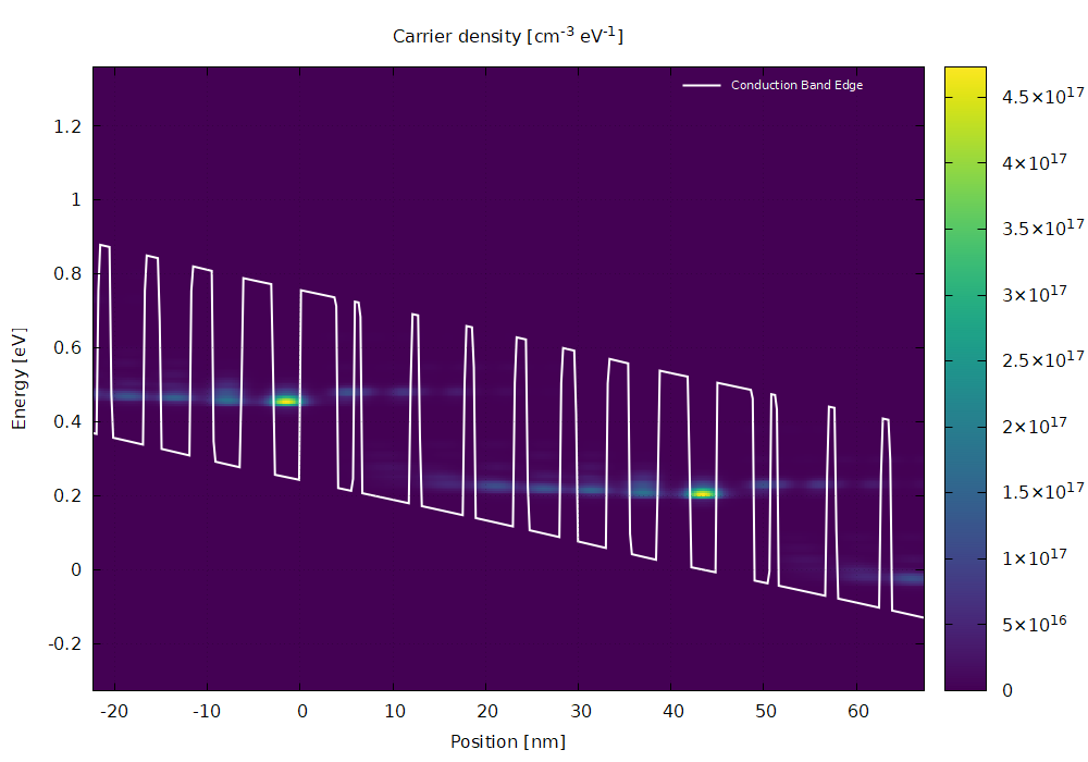
Figure 10 (a) Local density of states (LDOS) and (b) carrier density calculated at zone center#
The 2D current density map is shown in Figure 11 at zone center and with dispersion, i.e. integrating over the in-plane dispersion.
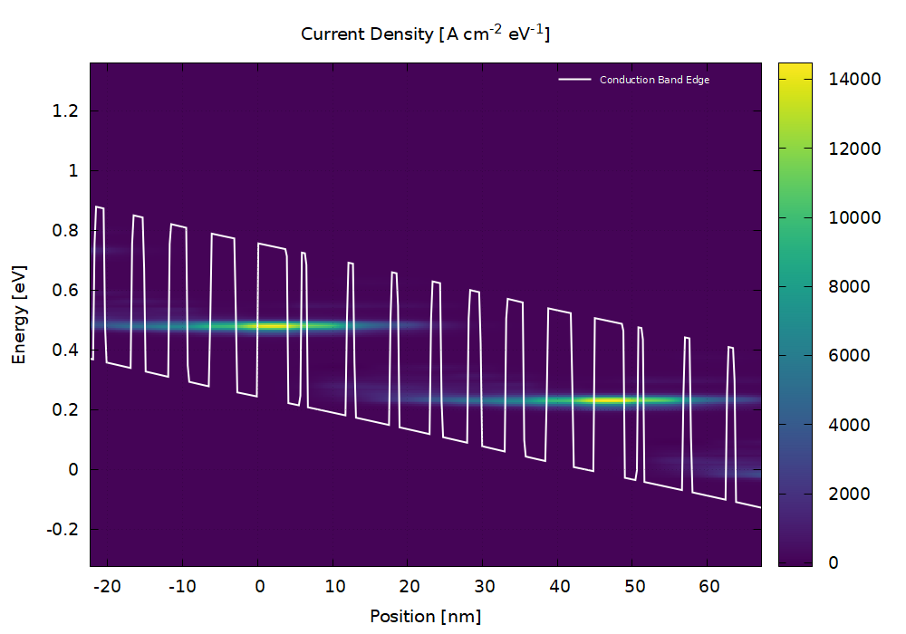
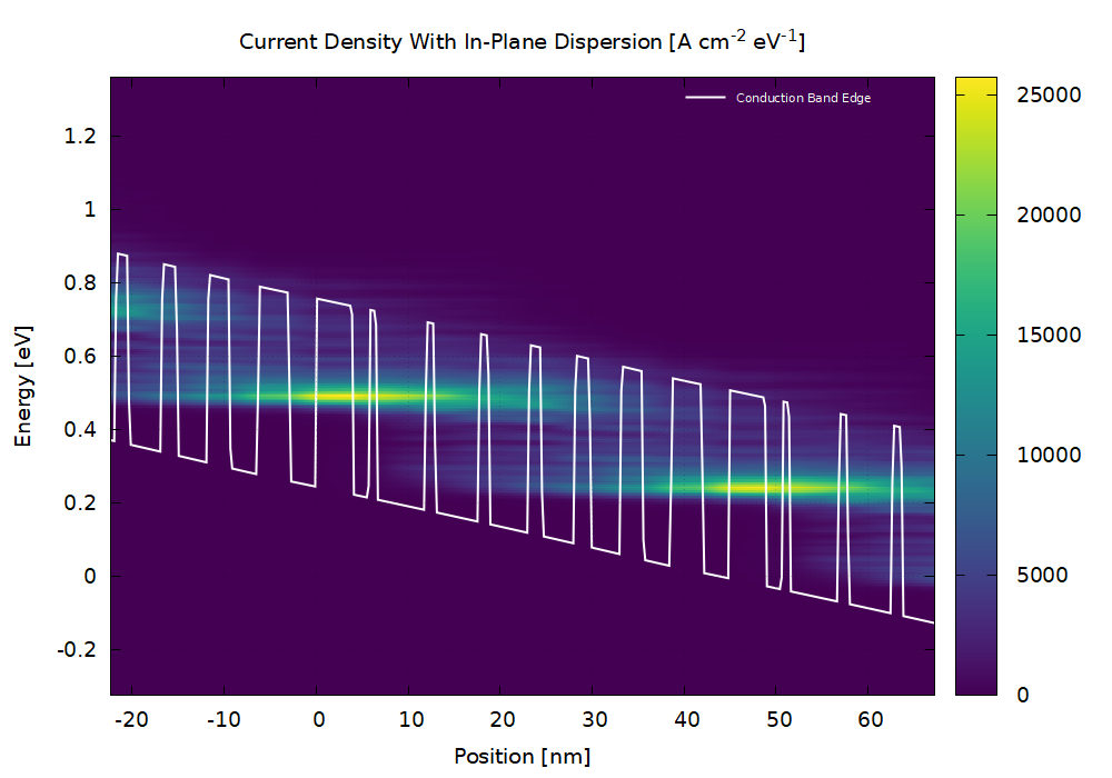
Figure 11 Current Density (a) at zone center and (b) with dispersion#
Gain/absorption spectrum#
The optical gain is calculated after the main NEGF solver for each bias point when the section Gain{ } is present in the input file. For each bias voltage, a gain/absorption spectrum is obtained as shown in Figure 12 . The recommended settings for QCLs is to use the self-consistent NEGF method (see GainMethod) To get more insight at which place gain/absorption occurs in the QCL, a position-resolved gain spectrum is also output.
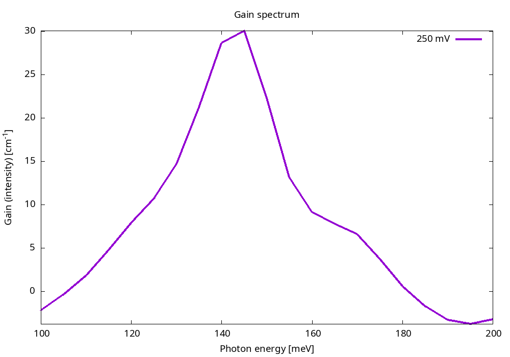
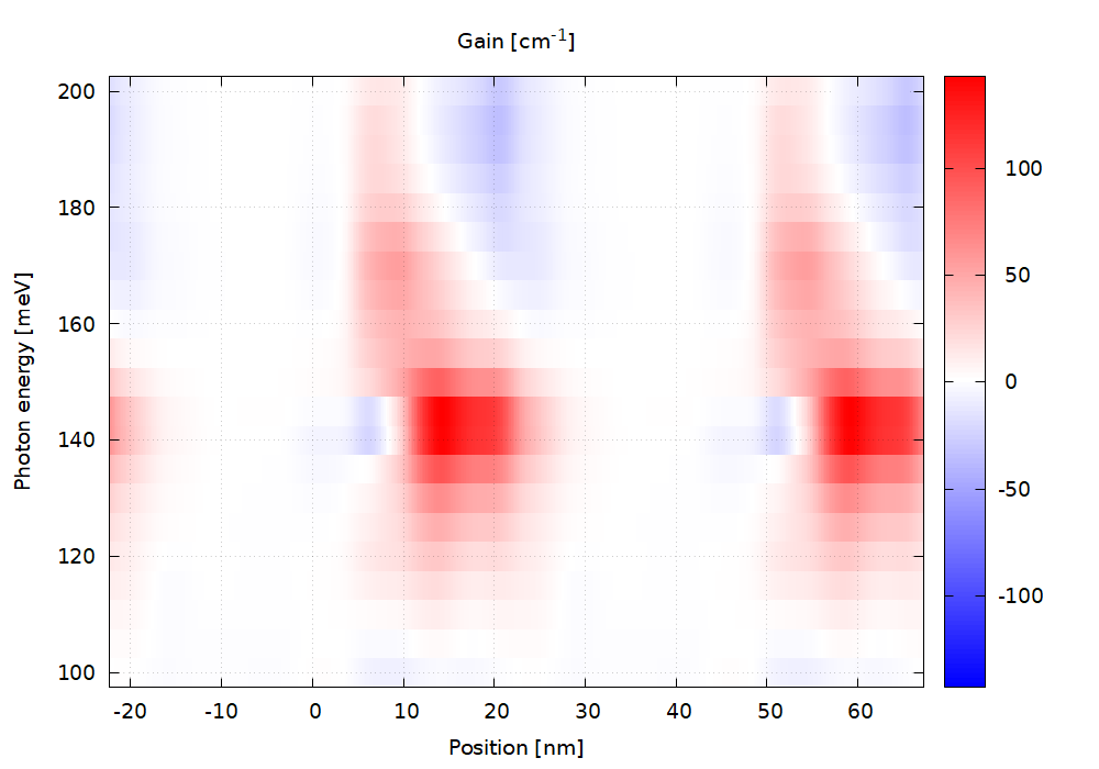
Figure 12 (a) Position-resolved gain spectrum and (b) position-resolved gain spectrum calculated using the self-consistent NEGF method.#
When a voltage sweep is performed, the maximum gain as a function of voltage is obtained (Figure 13). This figure gives also the position of the gain peak as a function of voltage.
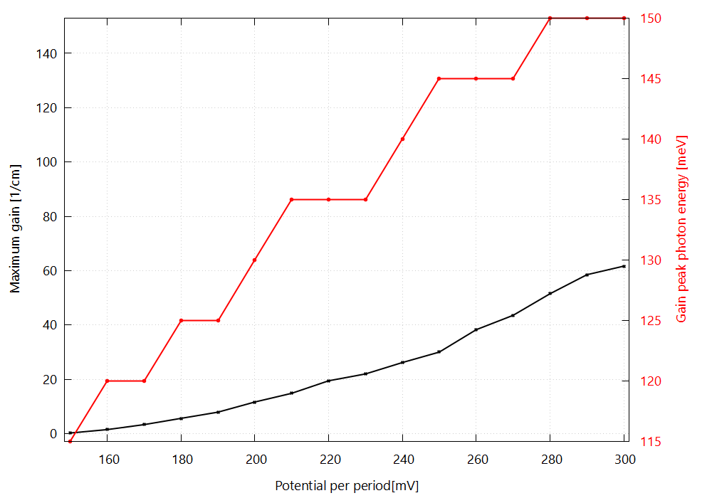
Figure 13 Maximum gain (left vertical axis) and photon energy at maximum gain (right vertical axis) as a function of voltage drop per period.#
Energy eigenstates in energy and tight-binding basis#
After the NEGF solver, the energy eigenstates are calculated including the computed electrostatic field (Figure 12)
In addition, when the AnalysisSeparator{ } command is defined in the input file, the QCL periodic structure can be divided in modules. For example, here a separator is defined only at the injection barrier. Then the tight-binding basis is defined as eigenstates of the Hamiltonian in modules located between two consecutive injection barriers.
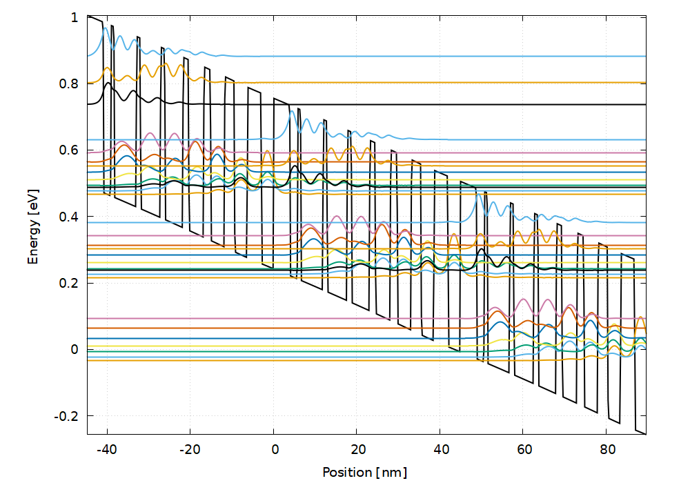
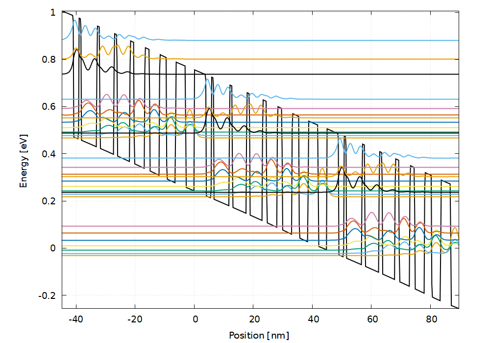
Figure 14 (a) Energy eigenstates and (b) tight-binding states computed after the NEGF solver and accounting for the electrostatic field.#
Further outputs in each of these basis include:
the populations and density matrix extracted from the lesser Green’s function
the dipoles and oscillator strength
the lifetimes and scattering rates computed from Fermi golden rule
the spectral function and the energy-resolved carrier distribution extracted from the lesser and retarded Green’s functions respectively.
the effective electronic temperature in each subband
Simulation of lasing above threshold#
When the command GainClamping is activated in the input file, together with the definition of the cavity mode by EMfield{ }, stimulated emission and absorption processes are accounted directly in the NEGF self-consistent loop. (see NEGF formalism and Photon-assisted transport)
Figure 15 shows the difference in I-V characteristics when gain clamping is considered. Below lasing threshold, the transport is governed by the non-radiative scattering mechanisms, as well as tunneling. Above lasing threshold, stimulated emission acts as an additional scattering mechanism (photon-induced transport), hence increasing the current density.
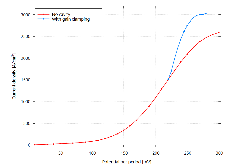
Figure 15 Current-voltage characteristics with and without gain clamping considered#
In Figure 16 (a), the net internally generated power is shown as the difference between stimulated emission and absorption processes.
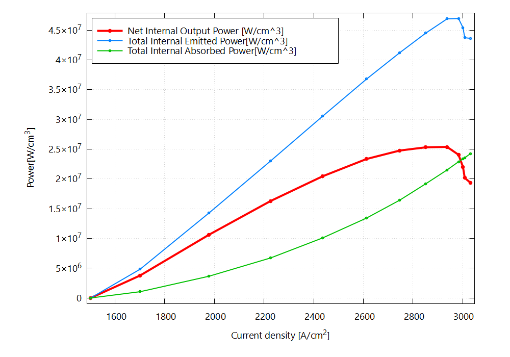
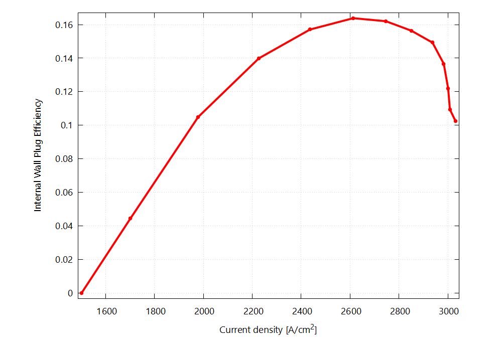
Figure 16 (a) Light-Intensity characteristic: the net internal output power is the difference between stimulated emission and absorption processes. (b) The internal wall-plug efficiency (WPE) is shown as a function of current density.#
QCL examples#
The following mid-IR QCL input file examples ([BismutoAPL2010], [BaiNatPhot2010], [BaiAPL2011]) are provided in the nextnano.NEGF software:
For this example, 3 sample files are provided
MidIR_QCL_InGaAs_InAlAs_Bismuto_APL2010.negf: simulates the I-V and gain without lasing (no gain clamping).
MidIR_QCL_InGaAs_InAlAs_Bismuto_APL2010_GainClamping.negf : similar input file but with lasing (with gain clamping)
Figure 17 compares the simulation time for the above input files as a function of the number of threads used (see NMaxThreads for setting the number of thhreads in the input file and/or customized nextnanomat performance settings).
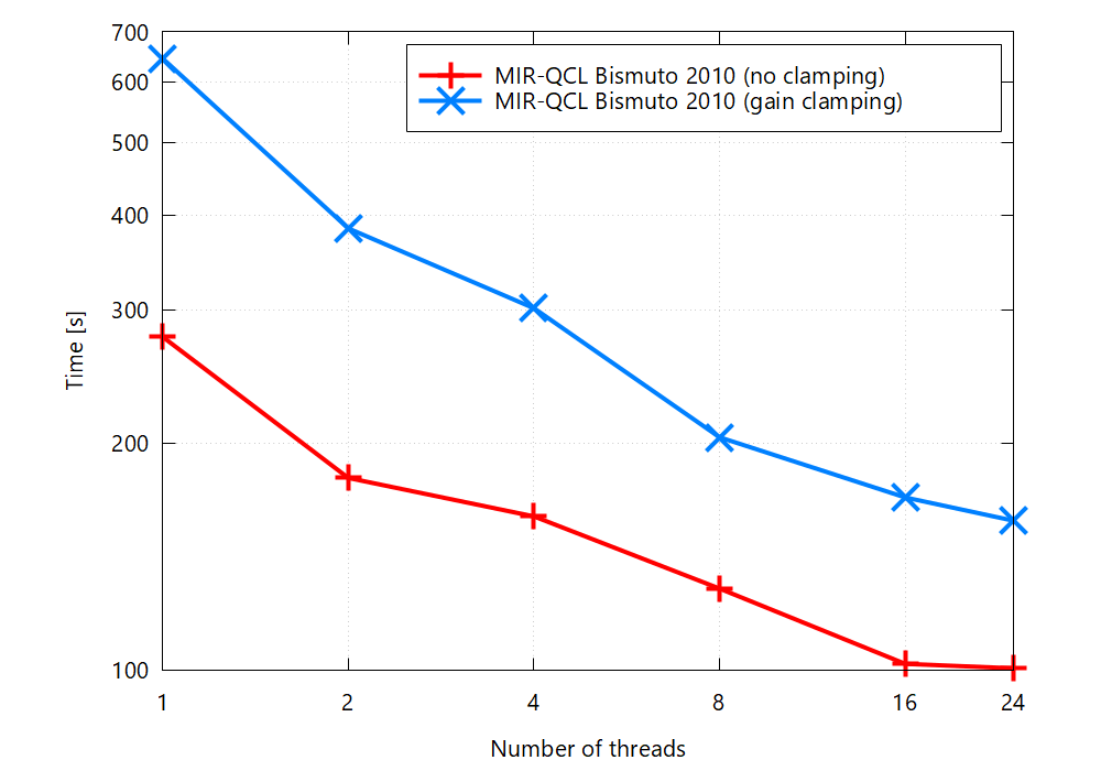
Figure 17 Simulation time per bias point vs number of threads for the input file [BismutoAPL2010]. The test was made using nextnano.NEGF version 2.0.3 on an Intel Core Ultra 9 285K.#