5.6.11. Non-resonant photoluminescence of GaAs/AlGaAs QWs
Attention
Input files for this tutorial has been recently modified and are not yet released. Please contact our nextnano support team to learn about their availability.
Warning
The new input file is prepared only for 300 K. Other temperatures will be included soon.
Header
- Files for the tutorial located in nextnano++\examples\quantum_wells
PL_non-resonant_QW_III-V.nnp
- Output Files:
bias_00000\Optics\spont_emission_power_region_longitudinal_nm.dat
- Scope:
In this tutorial, we show an approach how to model photoluminescence (PL) in 1D QW structures. The following is covered:
Short overview of the most essential groups which are needed in the input file for PL simulations
How to compute the absorption spectrum, when no experimental data is available
Results: photoluminescence spectra
Limitations of the simulation
- Important keywords:
Introduction
This tutorial shows approximate simulations of non-resonant photoluminescence of a quantum well in stationary conditions. Light impinges on the surface of the structure parallel to the growth direction. In this case, all the light is absorbed in the continuum of states in one of the barriers, away from the quantum well. Optical spectra calculated in a semi-classical approach are used here, which should be a decent approximation for the bulk material. Generation rates are calculated automatically and further used to calculate currents which pumps the quantum well where they can recombine. This part is done semi-classically. Later teh system involving Schrödinger equation is solved and, at the final stage, the Fermi’s golden rule is used to model emission spectrum of the pumped QW.
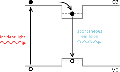
Figure 5.6.11.1 Visualization of involved processes: light absorption and generation of electron - hole pairs, trapping of carriers inside the quantum well, recombination and spontaneous emission of light
In the simulation a light source with Gaussian spectrum with central wavelength \(\lambda\)peak = 530 nm (2.34 ev) and linewidth of 10 meV is used. The intensity \(\Phi\)intensity is varied between the two values 0.5 \(\cdot\) 104 W/cm2 and 0.05 \(\cdot\) 104 W/cm2. The temperature in this simulation is swept between the three values 200 K, 250 K and 300 K.
The quantum well structure under consideration in this tutorial consists of 500 nm Al0.36Ga0.64 As cap barrier, 7 nm GaAs QW, 500 nm Al0.36Ga0.64 As second barrier, and 1000 nm GaAs substrate.
Keywords
The optical phenomena related to the irradiation, absorption and spontaneous emission processes, which should be taken into account in the simulation, have to be specified in the optics{ } block.
The spontaneous emission is calculated with quantum_spectra{}.
The absorption spectrum used in the group irradiation{} is calculated by semiclassical_spectra{}.
Inside the group classical{ } one has to specify energy resolved densities n(x,E) and p(x,E), which
are required for the semiclassical absorption and emission spectra. More information on the underlying
equations can be found here
To calculate the quantum mechanical emission spectra, one has to include the group quantum{ }. The group quantum{ } as well as current{} and poisson{ } are also required for self-consistent quantum-current-poisson calculations. Inside these group proper convergence parameters have to be chosen.
In this part, one has to think about proper convergence parameters for the solvers.
poisson{ ... }
currents{ ... }
quantum{ ... }
Note that proper boundary conditions are needed for Poisson and current equation. These are imposed by contact regions.
In our simulation, we apply ohmic{} contacts only to the bottom of the substrate, i.e. to the not illuminated side of the structure.
contacts{
    ohmic{ name = "whatever" bias = 0.0 }
}
Results
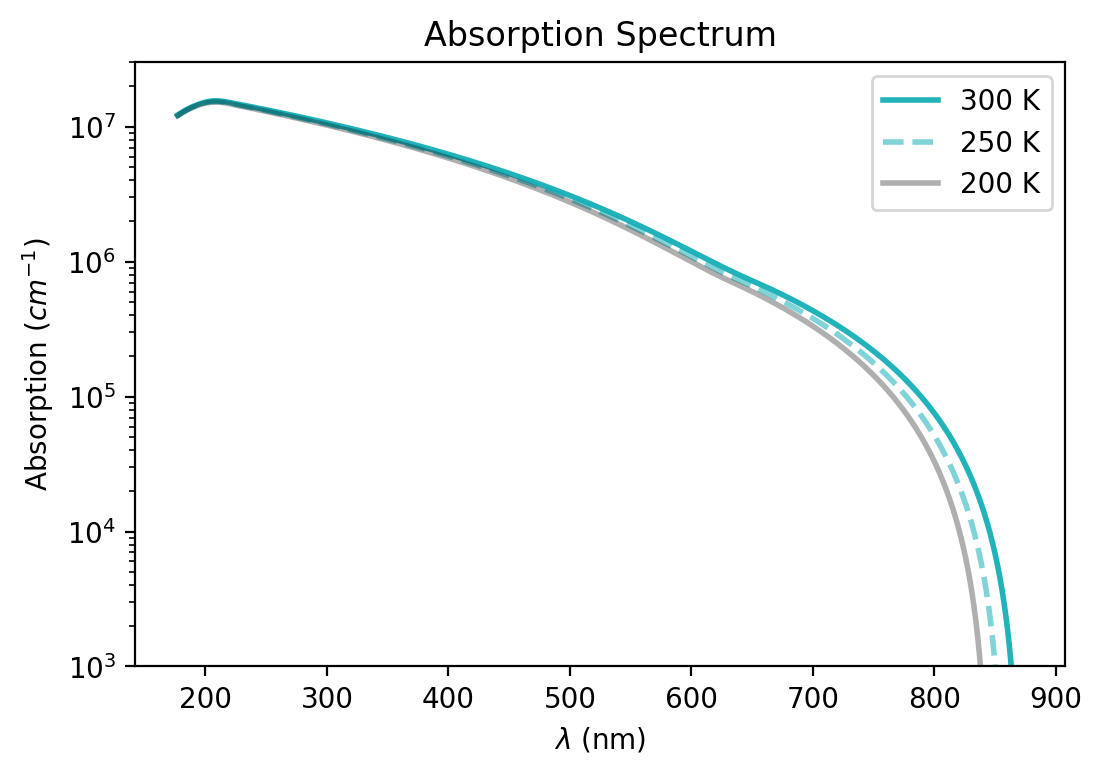
Figure 5.6.11.2 Calculated absorption spectrum
Now we can run the main input file 1D_PL_of_QW_nnp.nnp, which imports and uses the computed absorption spectrum.
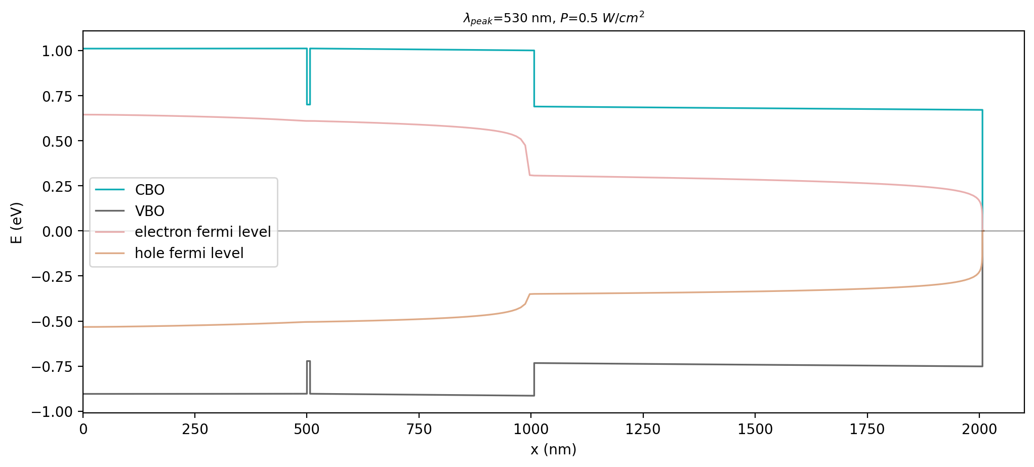
Figure 5.6.11.3 Energy profiles of conduction band (CBO) and valence band (VBO), with electron- and hole-Fermi levels across the structure
Figure 5.6.11.4 illustrates the spatial and energy distribution of electrons and holes with respect to the band edges for case: Pillumination 0.5 \(\cdot\) 104 W/cm2 at 300 K. Both, electrons and holes, are localized inside the quantum well, thus exhibit discrete energy levels. The occupation of the energy levels gives us insight about possible transitions (recombination) between electron states in the conduction band and hole states in the valence band. From Figure 5.6.11.4 we can deduce that most transition energies are in the interval 1.4eV-1.6eV of magnitude. For the emission spectrum, we assume to find its peak energy in this energy interval.
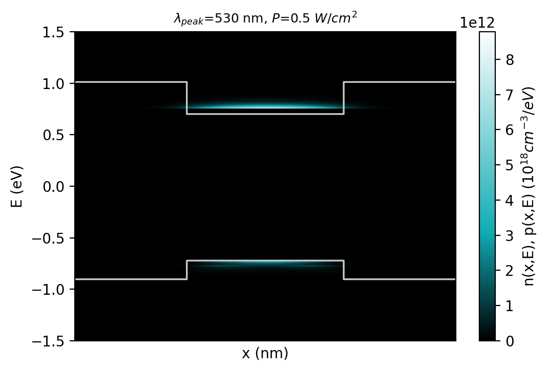
Figure 5.6.11.4 Electron density n(x,E) and hole density p(x,E) with conduction and valence band edges at 300K.
Figure 5.6.11.5 depicts the spatial and energy resolved generation rate inside the structure for the case: Pillumination 0.5 \(\cdot\) 104 W/cm2 at 300 K.
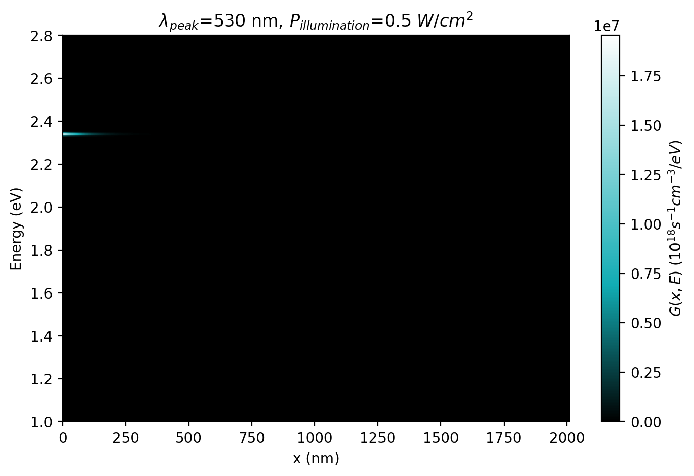
Figure 5.6.11.5 Photogeneration rate \(G(x, E)\) at \(T = 300 K\) and \(P = 0.5 \cdot 10\) 4 W/cm2
Figure 5.6.11.6 shows the normalized spontaneous emission spectra at different temperatures. The peak of the emission spectra are primarily attributed to the Ee1 - Eh1 transition inside the quantum well. Due to band gap shrinking the peak shifts to higher wavelengths with increasing temperatures. At higher temperatures the contribution from other transitions, such as Ee2 - Eh1 to the spectra becomes visible. Thus, the spectrum exhibit a broadening.
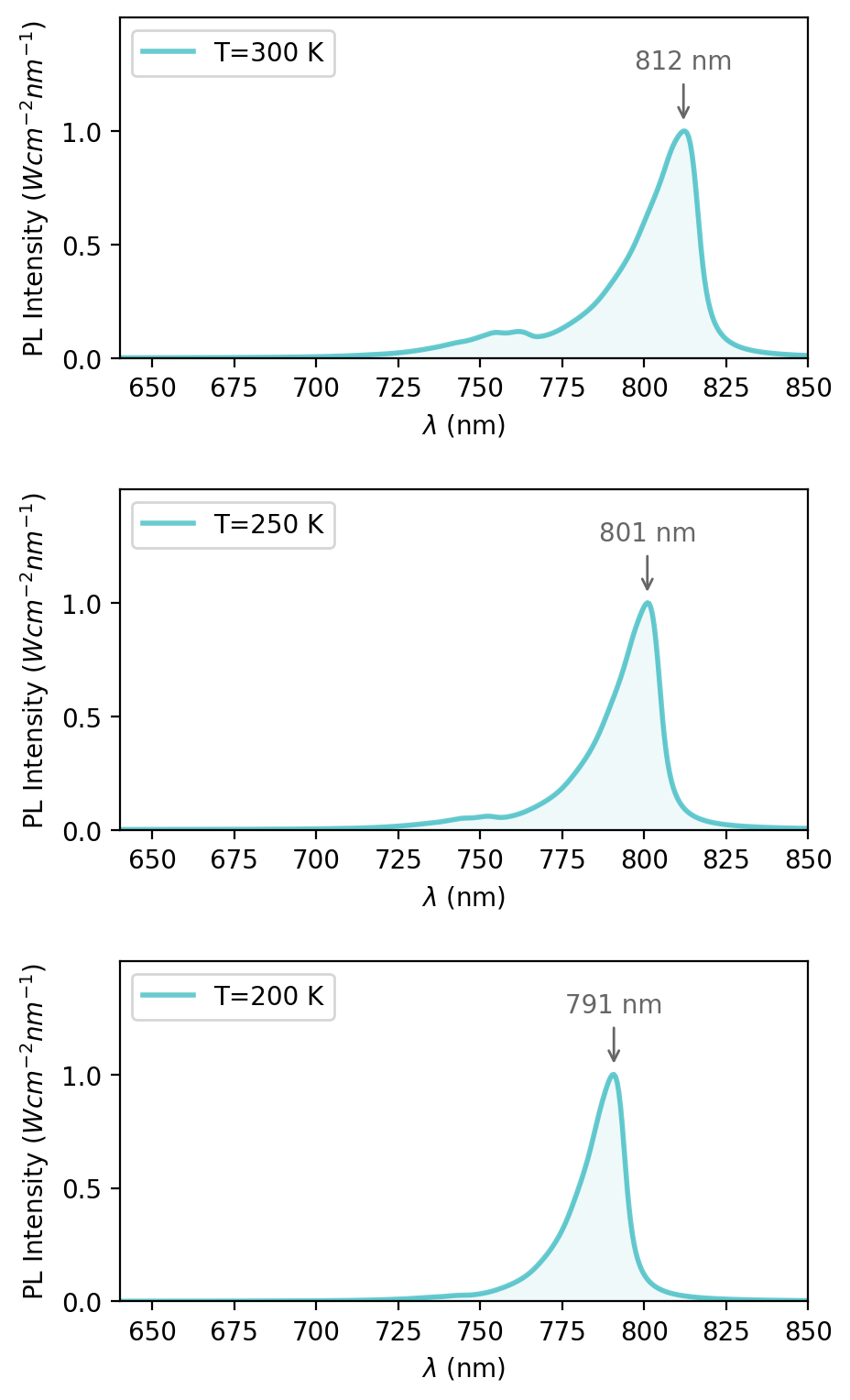
Figure 5.6.11.6 Normalized luminescence spectra with highlighted peak wavelength at each temperature (200 K, 250 K and 300 K), when illuminated by P = 0.5 \(\cdot\) 104 W/cm2.
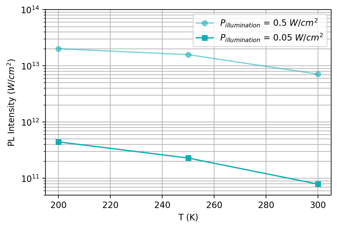
Figure 5.6.11.7 Total emitted intensity as a function of temperature.
Last update: 2025-10-23